
Preparation method of CaSi nanowires

A pretreatment, silicon substrate technology, applied in the direction of nanotechnology, nanotechnology, chemical instruments and methods, etc., can solve the problems of difficulty in forming one-dimensional CaSi nanowire structure, poor performance of CaSi nanostructure, and easy agglomeration and winding of nanowires. Achieve the effect of promoting effective transmission, excellent distribution uniformity and uniform diameter

Active Publication Date: 2021-03-30
CHONGQING UNIV OF ARTS & SCI
View PDF6 Cites 0 Cited by
  • Summary
  • Abstract
  • Description
  • Claims
  • Application Information

AI Technical Summary

Problems solved by technology

Secondly, it is difficult to form a one-dimensional CaSi nanowire structure, and it is easy to transform into a two-dimensional film structure during the preparation process.
In addition, the nanowires prepared by the existing preparation methods are easy to agglomerate and entangle or only generate short rod structures with large diameters, and the uniformity is poor, which makes the performance of the synthesized CaSi nanostructures poor.

Method used


Image

  • Preparation method of CaSi nanowires
  • Preparation method of CaSi nanowires
  • Preparation method of CaSi nanowires

Examples


Embodiment 1

[0031] A preparation method of CaSi nanowires, carried out as follows:

[0032] (1) Substrate pretreatment

[0033] Soak a monocrystalline silicon substrate with a size of 8mm*8mm, a thickness of 1mm, and a crystal plane of (111) in 50mL of acetone solution for ultrasonication, evaporate until at least 15mL of acetone solution remains, and then add hydrofluoric acid with a mass fraction of 50%, Soak nitric acid and acetic acid in a mixed solution with a volume ratio of 1:1:2 for 10 seconds, rinse with pure water, and finally dip with an 8% hydrofluoric acid aqueous solution, and dry in the air after washing;

[0034] (2) Preparation of nanowires

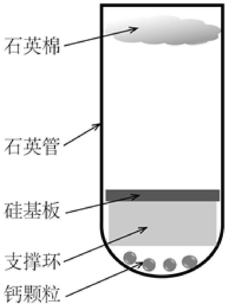
[0035] A. Place 0.025g of calcium granules on the bottom of the quartz container, place the silicon substrate in step (1) above the calcium granules, face down, with a distance of 5mm from the calcium granules, and place a small amount of quartz wool on the top of the container;

[0036] B. Put the quartz container in a vacuum, the...

Embodiment 2

[0039] A preparation method of CaSi nanowires, carried out as follows:

[0040] (1) Substrate pretreatment

[0041] Soak a monocrystalline silicon substrate with a size of 8mm*8mm, a thickness of 1mm, and a crystal plane of (111) in 50mL of acetone solution for ultrasonication, evaporate until at least 15mL of acetone solution remains, and then add hydrofluoric acid with a mass fraction of 50%, Soak nitric acid and acetic acid in a mixed solution with a volume ratio of 1:1:2 for 10 seconds, rinse with pure water, and finally dip in a hydrofluoric acid aqueous solution with a volume fraction of 5%, and dry in the air after washing;

[0042] (2) Preparation of nanowires

[0043] A. Place 0.02g of calcium particles on the bottom of the quartz container, place the silicon substrate in step (1) above the calcium particles, face down, and place a distance of 6mm from the calcium particles, and place a small amount of quartz wool on the top of the container;

[0044] B. Put the qua...

Embodiment 3

[0047] A preparation method of CaSi nanowires, carried out as follows:

[0048] (1) Substrate pretreatment

[0049] Soak a monocrystalline silicon substrate with a size of 8mm*8mm, a thickness of 1mm, and a crystal plane of (111) in 50mL of acetone solution for ultrasonication, evaporate until at least 15mL of acetone solution remains, and then add hydrofluoric acid with a mass fraction of 50%, Nitric acid and acetic acid are soaked in a mixed solution composed of 1:1:2 by volume for 10 seconds, rinsed with pure water, and finally dipped in hydrofluoric acid aqueous solution with a volume fraction of 10%, and dried in the air after washing;

[0050] (2) Preparation of nanowires

[0051] A. Place 0.03g of calcium granules on the bottom of the quartz container, place the silicon substrate in step (1) above the calcium granules, face down, with a distance of 4mm from the calcium granules, and place a small amount of quartz wool on the top of the container;

[0052] B. Put the q...


PUM

PropertyMeasurementUnit
Lengthaaaaaaaaaa
Lengthaaaaaaaaaa

Abstract

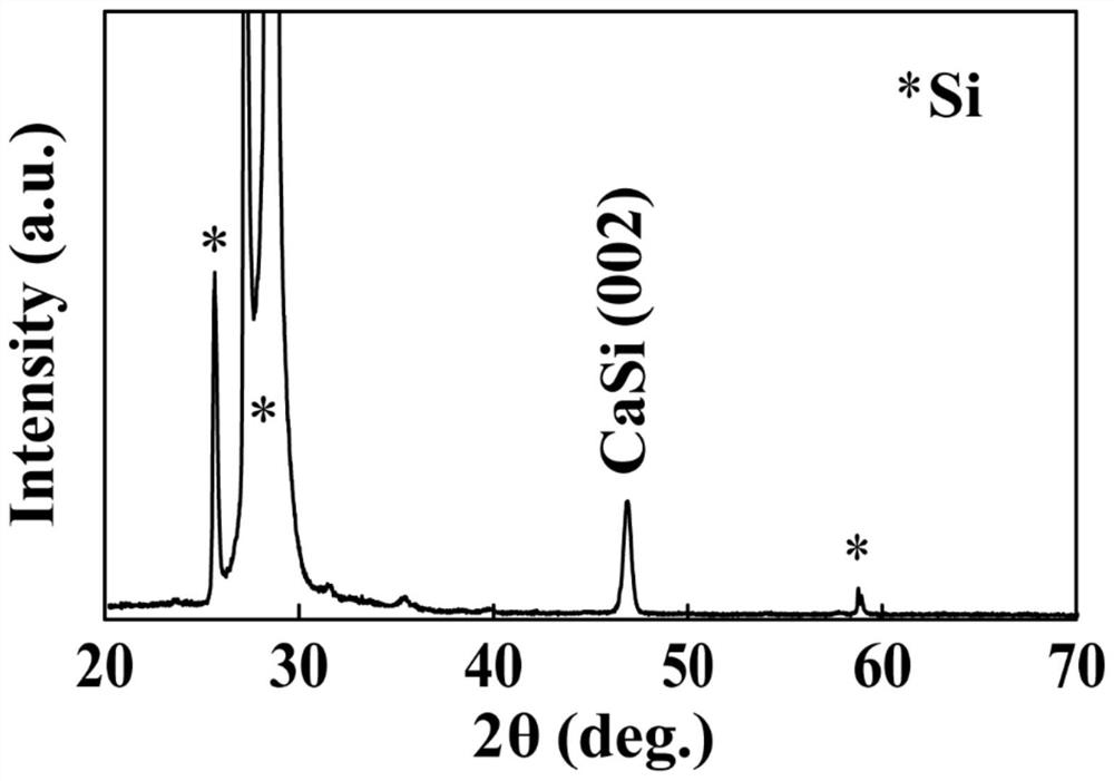
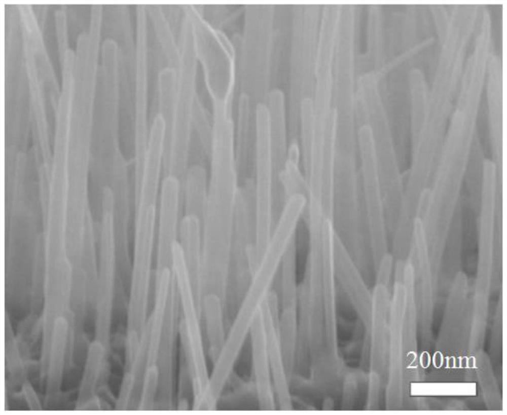
The invention relates to a preparation method of CaSi nanowires, wherein the preparation method comprises the steps: pretreating a monocrystalline silicon substrate with a crystal face (111), placingthe pretreated monocrystalline silicon substrate in a quartz container without contacting with calcium, placing the pretreated silicon substrate above calcium, placing a small amount of quartz wool atan opening of the container, heating the quartz container in vacuum to 630-690 DEG C, carrying out heat preservation reaction, and quickly cooling to room temperature. Other silicide impurity phasesare not generated in the product prepared through one-step reaction, the product is single-phase CaSi monocrystalline nanowires, the purity is high, the CaSi nanowires are perpendicular to the monocrystalline silicon substrate of the crystal face (111), the agglomeration and winding phenomena are avoided, the distribution uniformity is excellent, the density is large, the particle size is controlled between 30-50 nm, and the grown nanowires are uniform in diameter, can effectively adapt to large volume change without pulverization, have excellent electrical contact and conductivity, have a uniform one-dimensional structure, and promote effective transmission of charges; each nanowire is basically vertical to the substrate, does not agglomerate, enhances the conductivity, and does not needto be additionally added with an adhesive or a conductive agent.

Description

technical field [0001] The invention relates to the technical field of nanomaterials, in particular to a preparation method of CaSi nanowires. Background technique [0002] Semiconductor silicides are widely used in many industrial fields, such as the constituent materials of electric heating elements and integrated circuits. Most of the elements contained in silicides are non-toxic and environmentally friendly elements with abundant earth content. At the same time, because they naturally contain silicon elements, they have broader application prospects in silicon-based industries. In recent years, breakthroughs have been made in the research of semiconductor silicides in the fields of thermoelectric conversion, lithium batteries, and photoelectric detection. [0003] CaSi itself has a CrB structure, has a very small band gap (0.5eV), exhibits certain metallic properties, and has a very high melting point (1320°C). Recent research results show that CaSi has good hydrogen a...

Claims


Application Information

Patent Timeline
IPC IPC(8): C01B33/06B82Y30/00B82Y40/00C30B1/10C30B29/10
CPCC01B33/06B82Y30/00B82Y40/00C30B1/10C30B29/10C01P2002/72C01P2004/03C01P2004/64
Inventor 孟祥程江廖小青李璐立冈浩一
Owner CHONGQING UNIV OF ARTS & SCI
Learn More