Method for forming semiconductor device

A semiconductor and device technology, applied in the field of semiconductor device formation, can solve the problems of reducing the interface state of the gate oxide layer, reducing the probability of carrier trapping, etc., and achieve the effects of reducing silicon dangling bonds and suppressing thermionic effect.

Inactive Publication Date: 2012-06-06
SEMICONDUCTOR MANUFACTURING INTERNATIONAL (BEIJING) CORP
View PDF7 Cites 7 Cited by
  • Summary
  • Abstract
  • Description
  • Claims
  • Application Information

AI Technical Summary

Problems solved by technology

However, these improvements do not involve reducing the probability of carrier capture in the gate oxide layer, that is, how to effectively reduce the interface state in the gate oxide layer, mainly to reduce the interface traps for trapping carriers

Method used


Image

  • Method for forming semiconductor device
  • Method for forming semiconductor device
  • Method for forming semiconductor device

Examples


Embodiment Construction

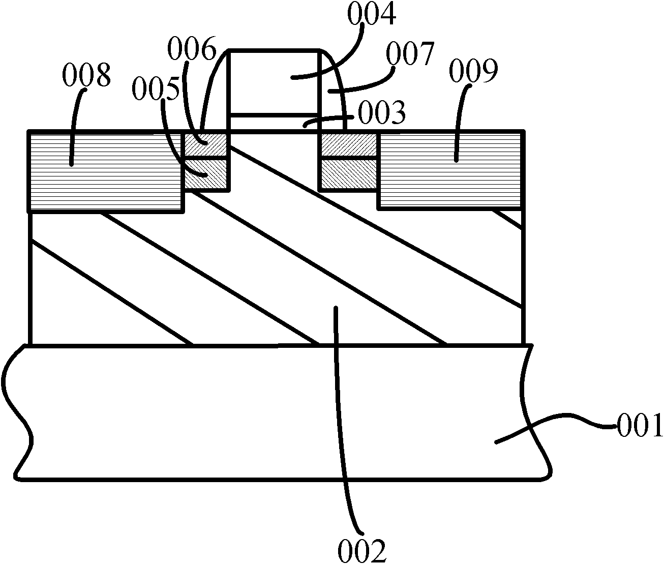
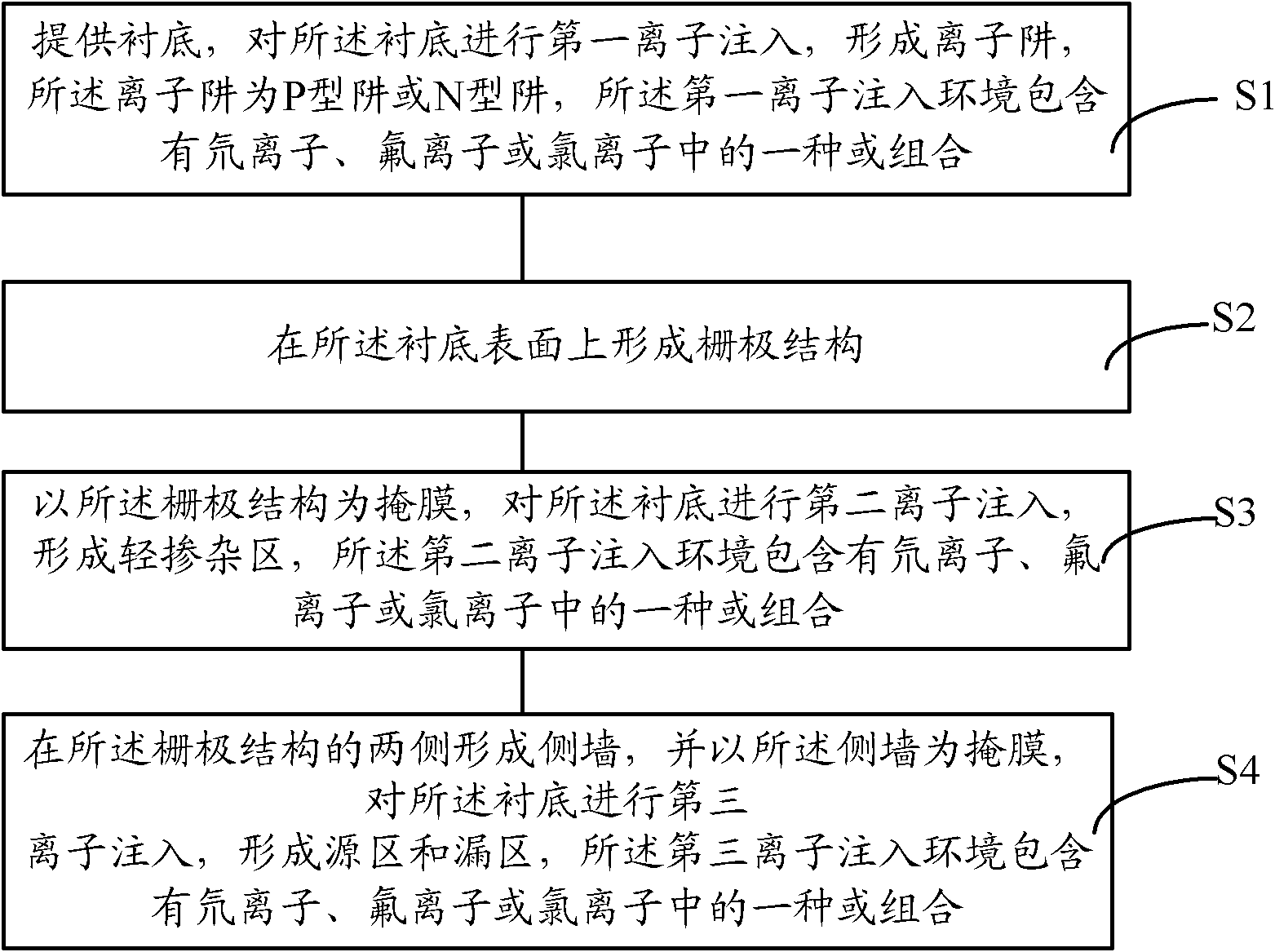
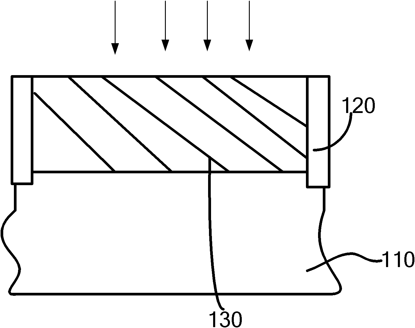
[0034] The present invention provides a method for forming a semiconductor device, which includes providing a substrate, performing a first ion implantation on the substrate to form an ion trap; forming a gate structure on the surface of the substrate; taking the gate structure as Mask, perform a second ion implantation on the substrate to form a lightly doped region, including a lightly doped source region and a lightly doped drain region; form sidewalls on both sides of the gate structure, and use the The sidewall is a mask, and a third ion implantation is performed on the substrate to form a heavily doped region, including a heavily doped source region and a heavily doped drain region; wherein the first ion implantation environment and the second ion implantation environment One ion implantation environment or multiple ion implantation environments in the third ion implantation environment also contains one or a combination of deuterium ions, fluoride ions, or chloride ions. ...


PUM


Abstract

The invention provides a method for forming a semiconductor device, comprising the following steps of: providing a substrate, carrying out first ion implantation on the substrate and forming an ion trap; forming a grid structure on the surface of the substrate; taking the grid structure as a mask, carrying out second ion implantation on the substrate and forming lightly-doped regions comprising lightly-doped source regions and lightly-doped drain regions; forming side walls at the two sides of the grid structure, taking the side walls as masks, carrying out third ion implantation on the substrate and forming heavily-doped regions comprising heavily-doped source regions and heavily-doped drain regions, wherein one or more of a first ion implantation environment, a second ion implantation environment and a third ion implantation environment also comprise one or combination of deuterium ions, fluorine ions or chloride ions. According to the method, the deuterium ions, the fluorine ions or the chloride ions are used for saturating silicon dangling bonds at the interface position between the substrate and the grid structure, so as to restrain the hot electron effect.

Description

Technical field [0001] The present invention relates to the field of semiconductor manufacturing, and in particular to a method for forming semiconductor devices. Background technique [0002] The main device in integrated circuits, especially VLSIs, is Metal Oxide Semiconductor (MOS). Since the invention of the integrated circuit, its performance and function have advanced by leaps and bounds, and the geometric size of the MOS device has been continuously shrinking, and its feature size has now entered the nanometer scale. [0003] In the process of scaling down the MOS device, the drain voltage does not decrease, which leads to an increase in the electric field in the channel region between the source and the drain. Under the action of a strong electric field, electrons are in between two collisions. It will accelerate to a speed many times higher than the thermal motion speed, so the kinetic energy is very large. These electrons are called hot electrons, and the hot electrons a...

Claims


Application Information

Patent Timeline
Patent Type & Authority Applications(China)
IPC IPC(8): H01L21/336H01L21/265
Inventor 何永根卢炯平陈志豪
Owner SEMICONDUCTOR MANUFACTURING INTERNATIONAL (BEIJING) CORP
Why Eureka
Try Eureka