Laser machining method for matching with light-emitting diode (LED) inner cutting process

A laser processing method and internal cutting technology, applied in laser welding equipment, metal processing equipment, manufacturing tools, etc., can solve the problems of reduced laser absorption and reduced processing efficiency.

Inactive Publication Date: 2012-06-20
SUZHOU DELPHI LASER
View PDF7 Cites 22 Cited by
  • Summary
  • Abstract
  • Description
  • Claims
  • Application Information

AI Technical Summary

Problems solved by technology

Because the metal film layer has a wide reflection spectrum, the commonly used solid-state laser wavelengths are all within its r...

Method used


Image

  • Laser machining method for matching with light-emitting diode (LED) inner cutting process
  • Laser machining method for matching with light-emitting diode (LED) inner cutting process
  • Laser machining method for matching with light-emitting diode (LED) inner cutting process

Examples


Embodiment 1

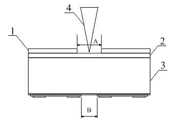
[0023] Step 1: If Figure 1a As shown, the laser light 4 is focused on the metal reflective film 1 to vaporize the metal reflective film 1 to form a trench A with a certain removal width. Before processing, use a high-precision image positioning system to strictly align the centerline of the groove A with a certain removal width with the centerline of the dicing line B reserved by the lithography on the front of the wafer. The laser processing parameters are controlled so that the distributed Bragg reflection film 2 at the bottom of the groove is not damaged, and no metal reflection film or dust remains in the groove A.

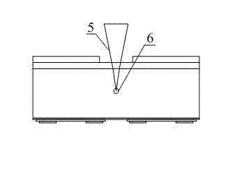
[0024] Step 2: If Figure 1b As shown, the internal cutting laser 5 is used to directly penetrate the distributed Bragg reflection film 2 in the trench and focus on the inside of the wafer to form an internal burst region 6, and form a linear array along the cutting direction.

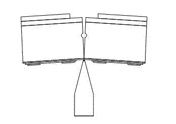
[0025] Step 3: If Figure 1c As shown, pressure is applied on the dicing line B...

Embodiment 2

[0028] Step 1: If Figure 2a As shown in , the laser light 4 is focused on the metal reflective film 1 and the distributed Bragg reflective film 2, and the metal reflective film 1 and the distributed Bragg reflective film 2 are vaporized to form a groove A with a certain removal width. Before processing, use a high-precision image positioning system to strictly align the centerline of the groove A with a certain removal width with the centerline of the dicing line B reserved by the lithography on the front of the wafer. Control the laser processing parameters so that the substrate surface at the bottom of the trench is not damaged and the front side of the wafer is not damaged. There is no metal reflective film or dust residue in groove A. When implementing this step, lasers of different types and parameters can also be used to remove the two reflective films respectively.

[0029] Step 2: If Figure 2b As shown, the inner burst zone 6 is formed by using the inner cutting l...


PUM


Abstract

The invention relates to a laser machining method for matching with a light-emitting diode (LED) inner cutting process. According to the laser machining method, metal reflecting films or distributed Bragg reflecting films or double-layer reflecting films which consist of the metal reflecting films and the distributed Bragg reflecting films are distributed on the reverse side of a wafer; laser is focused to the reflecting films, and laser beams and the wafer make relative motion, so that the single-layer reflecting films or one layer or two layers of double-layer reflecting films are removed by gasifying to form a groove; a central line of the groove aligns with that of a cutting way on the front of the wafer; and in the inner cutting process, inner cutting laser is focused inside the wafer by the groove to form an internal crack area and form a linear array along the cutting direction, and pressure is exerted on the cutting way on the front of the wafer, so that the wafer is cracked along the set cutting direction. The method is matched with the inner cutting process to cut the LED wafer, so the method has the characteristics of high speed, high accuracy, small damage to the surface of sapphire and the like.

Description

technical field [0001] The invention relates to a laser processing method matched with LED internal cutting processing, which is used for internal cutting processing of LED wafers. Background technique [0002] Most of the current large-scale commercial LED chips are based on sapphire, and sapphire has a wide spectral transmittance, ranging from ultraviolet to near infrared. Therefore, part of the light emitted by the light-emitting area on the LED chip will be emitted from the direction of the substrate. With the continuous improvement of the LED luminous efficiency requirements, collecting this part of the light overflowing from the back has become an important method to improve the LED luminous efficiency. And plating a broad-spectrum reflective film on the back has developed into one of the mature and economical methods. [0003] The back coating of sapphire-based LEDs generally has a multi-layer structure, and the contact layer with sapphire is a single-layer or multi-...

Claims


Application Information

Patent Timeline
IPC IPC(8): B23K26/40B23K26/04
Inventor 赵裕兴郭良
Owner SUZHOU DELPHI LASER
Why Eureka
Try Eureka