Composite integrated sensor structure and manufacture method thereof

A technology for integrating sensors and manufacturing methods, applied in microstructure technology, microstructure devices, manufacturing microstructure devices, etc., can solve problems such as increased production costs and incompatibility

Active Publication Date: 2012-06-20
ADVANCED SEMICON MFG CO LTD
View PDF5 Cites 17 Cited by
  • Summary
  • Abstract
  • Description
  • Claims
  • Application Information

AI Technical Summary

Problems solved by technology

These processes are the current mainstream, but they are not compatible with conventional semiconductor processes. Therefore, customized sensor processing production lines are required, which increases production costs.

Method used


Image

  • Composite integrated sensor structure and manufacture method thereof
  • Composite integrated sensor structure and manufacture method thereof
  • Composite integrated sensor structure and manufacture method thereof

Examples


Embodiment Construction

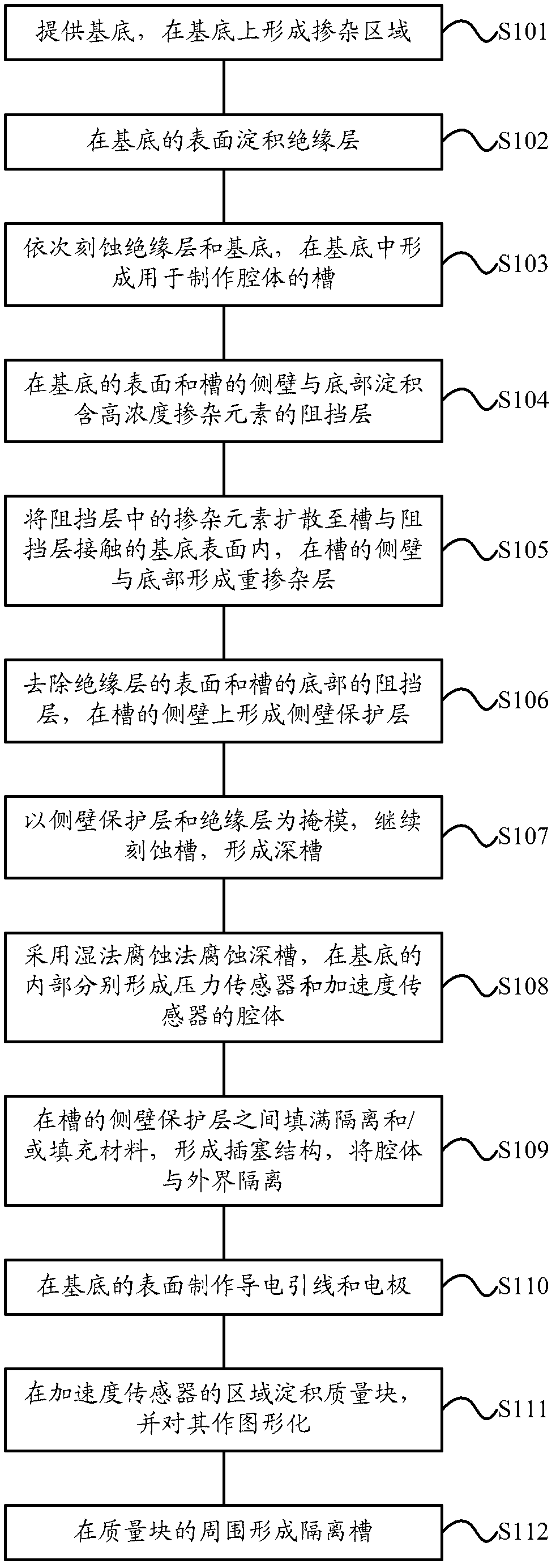
[0045] The present invention will be further explained below with reference to specific embodiments and drawings. In the following description, more details are set forth in order to fully understand the present invention. However, the present invention can obviously be implemented in many other ways than the description here. Those skilled in the art can make similar promotion and deduction according to actual application conditions without violating the connotation of the present invention. Therefore, the content of this specific embodiment should not limit the protection scope of the present invention.

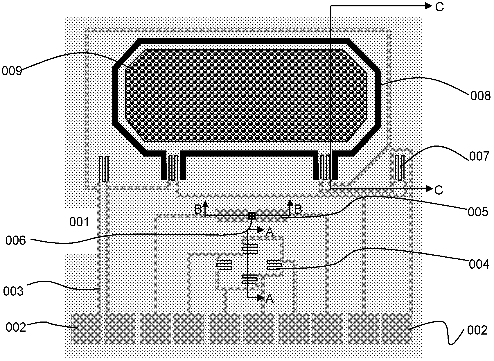
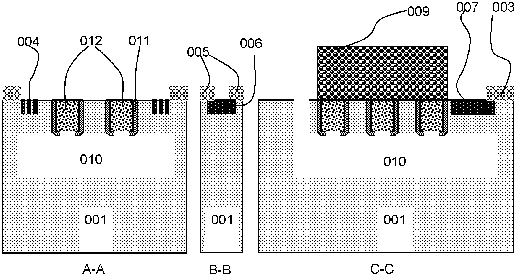
[0046] figure 1 It is a schematic plan view of a composite integrated sensor structure according to an embodiment of the present invention. As shown in the figure, you can see that this kind of composite integrated sensor structure contains an acceleration sensor (located in the upper half of the figure), a temperature sensor (located in the middle area of ​​the figure), and a ...


PUM


Abstract

The invention provides a composite integrated sensor structure and a manufacture method of the composite integrated sensor structure. The method comprises the following steps that: a substrate is provided, and a doping region is formed on the substrate; an insulating layer is deposited on the surface of the substrate; the insulating layer and the substrate are etched for forming grooves; a barrier layer with doped elements is deposited on the surface of the substrate and the bottom and the side wall of the grooves; the doped elements are diffused into the substrate to from a heavy doping layer; the barrier layer at the bottom of the grooves is removed, and a side wall protecting layer is formed on the side wall of the grooves; the grooves are continuously etched by using the side wall protecting layer and the insulating layer as masks, and deep grooves are formed; the deep grooves are corroded, a cavity is formed inside the substrate; isolation and / or filling materials are fully filled between side wall protecting layers; conducting leads and electrodes are manufactured on the surface of the substrate; a mass block is deposited in an acceleration sensor region and is graphical; and an isolation groove is formed on the periphery of the mass block, and the mass block is connected with the substrate in a cantilever mode. The composite integrated sensor structure and the manufacture method adopt a front-side process compatible with the conventional semiconductor process and have the advantages of practicability, economy, high performance and the like.

Description

Technical field [0001] The present invention relates to the technical field of micro-electromechanical system (MEMS) manufacturing. Specifically, the present invention relates to a composite integrated sensor structure integrating a temperature sensor, an acceleration sensor and a pressure sensor and a manufacturing method thereof. Background technique [0002] With the development of sensor technology, sensor chips no longer contain a single sensor device, but more appear in the form of a system-on-chip (SOC or SIP). In a system-on-chip, multiple sensor device units are often integrated, and even peripheral CMOS integrated circuits are included to form a systematic on-chip composite integrated sensor structure. The emergence of on-chip sensing systems has made the integration of sensors higher and higher, more powerful, and smaller and smaller, while the cost has also been significantly reduced. [0003] The structure and manufacturing method of the composite integrated sensor ar...

Claims


Application Information

Patent Timeline
Patent Type & Authority Applications(China)
IPC IPC(8): B81C1/00G01D21/02
Inventor 张挺薛维佳倪胜中谢志峰
Owner ADVANCED SEMICON MFG CO LTD
Why Eureka
Try Eureka