Flexible stainless steel substrate copper-indium-gallium-selenium film battery and preparation method thereof
A copper indium gallium selenide and thin-film battery technology, applied in the field of solar cells, can solve the problems of complicated equipment operation, skin explosion, battery peeling, etc., and achieve the effect of simplifying the preparation process
- Summary
- Abstract
- Description
- Claims
- Application Information
AI Technical Summary
Problems solved by technology
Method used
Image
Examples
Embodiment 1
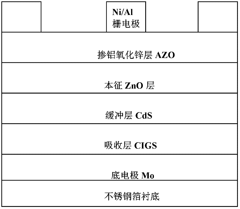
[0035] A method for preparing a copper indium gallium selenide thin film solar cell with a flexible stainless steel substrate, the steps are as follows:
[0036] 1) Put the SUS304 stainless steel foil with a thickness of 0.08mm into the vacuum chamber after ultrasonic cleaning, heat treatment at 400°C for 10 minutes, and the vacuum degree is 5×10 -4 Pa;
[0037] 2) Sputter the double-layer Mo back electrode by magnetron sputtering, the operating current is 1.2 amperes, the sputtering pressure of the first layer is 1.2 Pa, the thickness is 0.1 μm, the sputtering pressure of the second layer is 0.1 Pa, and the thickness is 1 μm;
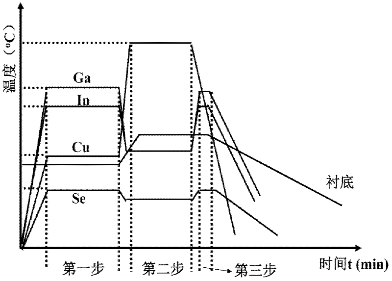
[0038] 3) Put the stainless steel substrate with the back electrode into the co-evaporation vacuum chamber at a vacuum degree of 6×10 -4 At Pa, degas the substrate at 400°C for 15 minutes, then increase the substrate temperature to 550°C, raise the temperature of the Se evaporation source furnace to 230°C, and anneal for 20 minutes in a Se atmosphere ...
Embodiment 2
[0045] A method for preparing a copper indium gallium selenide thin film solar cell with a flexible stainless steel substrate, the steps are as follows:
[0046] 1) Put the SUS304 stainless steel foil with a thickness of 0.08mm into the vacuum chamber after ultrasonic cleaning, heat treatment at 500°C for 10 minutes, and the vacuum degree is 5×10 -4 Pa;
[0047] 2) Sputter the double-layer Mo back electrode by magnetron sputtering, the operating current is 1.2 amperes, the sputtering pressure of the first layer is 1.2 Pa, the thickness is 0.1 μm, the sputtering pressure of the second layer is 0.1 Pa, and the thickness is 1 μm;
[0048] 3) Put the stainless steel substrate with the back electrode into the co-evaporation vacuum chamber at a vacuum degree of 6×10 -4 At Pa, degas for 15 minutes at a substrate temperature of 400°C, then raise the substrate temperature to 550°C, raise the temperature of the Se evaporation source furnace to 230°C, and anneal for 20 minutes in a Se a...
PUM
| Property | Measurement | Unit |
|---|---|---|
| Thickness | aaaaa | aaaaa |
| Thickness | aaaaa | aaaaa |
| Thickness | aaaaa | aaaaa |
Abstract
Description
Claims
Application Information


