Laser active detecting device based on MEMS (micro-electromechanical system) two-dimensional scanning mirror array

A technology of two-dimensional scanning mirror and active detection, which is applied in the direction of measuring device, electromagnetic wave re-radiation, radio wave measurement system, etc., can solve the problems of complex structure, low scanning speed and low work efficiency, and achieve high scanning frequency and high scanning efficiency. Effects with a large range and simple structure

Inactive Publication Date: 2012-06-27
XI AN JIAOTONG UNIV
View PDF3 Cites 11 Cited by
  • Summary
  • Abstract
  • Description
  • Claims
  • Application Information

AI Technical Summary

Problems solved by technology

[0006] It can be seen from the above table that mechanical scanning has a large scanning angle, is less affected by temperature, and is suitable for lasers of various wavelengths, but the scanning speed is low, the structure is complex, the volume, quality, and power consumption are relatively large, and the price of high-speed motors also more expensive
Acousto-optic scanning can obtain high working frequency, but the scanning deflection angle is small, the light loss is large, and the working efficiency is very low
[0007] MEMS two-dimensional scanning mirror is a good laser scanning device, but the scanning angle of a single MEMS two-dimensional scanning mirror is limited, which is greatly restricted in the application process. It is necessary to find a new large-scale scanning device

Method used


Image

  • Laser active detecting device based on MEMS (micro-electromechanical system) two-dimensional scanning mirror array
  • Laser active detecting device based on MEMS (micro-electromechanical system) two-dimensional scanning mirror array
  • Laser active detecting device based on MEMS (micro-electromechanical system) two-dimensional scanning mirror array

Examples


specific Embodiment approach

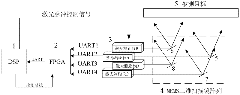
[0018] The DSP signal processing circuit 1 generates a laser pulse control signal to control the laser rangefinder array 3 to emit pulsed laser light. After the laser beam is scanned by the micromechanical (MEMS) two-dimensional scanning mirror array 4, it is irradiated on the detected target 5, and the laser beam is scanned. After being reflected back to the laser rangefinder, the laser rangefinder measures the distance of the measured target according to the time difference between the emitted laser pulse and the received laser pulse, and the DSP signal processing circuit 1 uses the control bus to control the FPGA logic circuit 2 to connect the micromachines ( MEMS) two-dimensional scanning mirror array 4 sets of laser range finder, read the measurement results into the DSP signal processing circuit 1, DSP signal processing circuit 1 sorts and generates the four sets of measurement results of the micromechanical (MEMS) two-dimensional scanning mirror array A 3D laser image of...


PUM


Abstract

The invention discloses a laser active detecting device based on an MEMS (micro-electromechanical system) two-dimensional scanning mirror array. A DSP (digital signal processor) signal processing circuit 1 is used for generating a laser pulse control signal to control a laser ranging device array to emit a pulse laser beam; after being scanned by the MEMS two-dimensional scanning mirror array, the laser beam is irradiated on a detected target; after the laser beam is reflected back to the laser ranging device array, the distance of the detected target is measured by the laser ranging device array according to a time difference between the laser pulse emission and the laser pulse receiving; and a control bus is utilized by the DSP signal processing circuit to control an FPGA (field programmable gate array) logic circuit to be respectively connected with four sets of laser ranging device arrays of the MEMS two-dimensional scanning mirror array, so as to read a measuring result into the DSP signal processing circuit. The device provided by the invention has the advantages of simple structure, high scanning speed, large scanning scope, low cost, small volume, light weight, and the like.

Description

technical field [0001] The invention relates to a laser detection device, in particular to a laser active detection device based on a micromachine (MEMS) two-dimensional scanning mirror. Background technique [0002] Laser detection technology has a history of more than 40 years. High-speed laser scanning technology has always been a bottleneck technology restricting the development of laser detection technology. Traditional laser scanning methods mainly include mechanical scanning and acousto-optic (electro) optical scanning, but these two scanning methods have certain limitations when used in laser active imaging guidance. Mechanical scanning is a relatively mature scanning technology, which uses the rotation or vibration of optical elements such as mirrors or transmission mirrors to change the propagation direction of the beam to achieve beam scanning. The acousto-optic (electro)-optic scanning uses the acousto-optic effect to change the propagation direction of the bea...

Claims


Application Information

Patent Timeline
Patent Type & Authority Applications(China)
IPC IPC(8): G01S17/02G01S17/89
Inventor 孙剑尤政张弛张潮史浩天
Owner XI AN JIAOTONG UNIV
Why Eureka
Try Eureka