Manufacturing method for planar bidirectional trigger diode chip

A bidirectional triggering and manufacturing method technology, which is applied in semiconductor/solid-state device manufacturing, electrical components, circuits, etc., can solve problems such as complex procedures, high cost, and unacceptable market, and achieve the effect of reducing fragmentation rate and high rebound voltage

Inactive Publication Date: 2012-06-27
佛山益辰电子科技有限公司
View PDF13 Cites 2 Cited by
  • Summary
  • Abstract
  • Description
  • Claims
  • Application Information

AI Technical Summary

Problems solved by technology

The process is extremely complicated, the cost is extremely high, and the market cannot accept it

Method used


Image

  • Manufacturing method for planar bidirectional trigger diode chip
  • Manufacturing method for planar bidirectional trigger diode chip
  • Manufacturing method for planar bidirectional trigger diode chip

Examples


Embodiment Construction

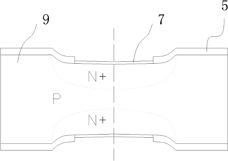
[0028] The present invention as Figure 1-11 Shown: using a P-type wafer 1 with a thickness of 100-300 μm as a raw material, the process of growing an oxide layer 2 on the surface of the wafer 1, a photolithographic diffusion window 3 and cutting the wafer 1 into chips 9, in the process of the photolithographic diffusion window 3 and The process of cutting the wafer 1 into chips 9 includes the following processes:

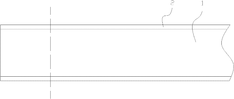
[0029] The aforementioned process of growing an oxide layer is as follows: figure 2 Shown: the cleaned P-type wafer 1 is grown at 1050°C with an oxide layer 2 as a diffusion mask;

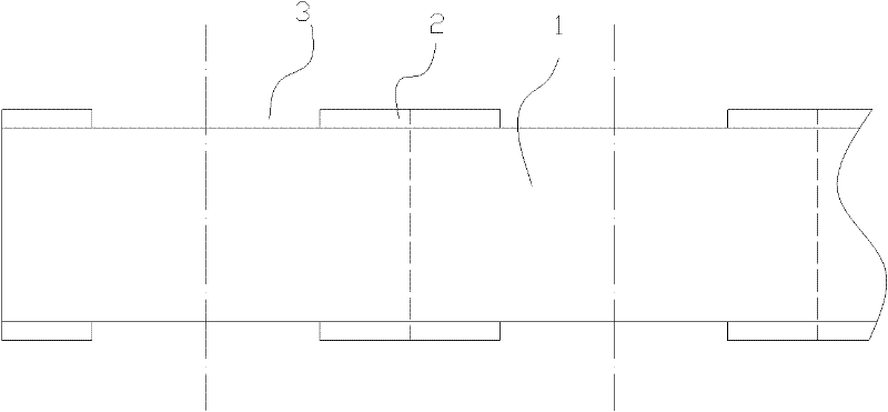
[0030] The process of forming diffusion window by photolithography is as follows: image 3 As shown, a part of the oxide layer 2 is removed on the surface of the wafer 1 by a photolithography process to leave a diffusion window 3 .

[0031] 1) Diffusion window sinks; such as Figure 4 After cleaning, inject mixed acid into the diffusion window 3 to corrode the surface of the wafer ...


PUM

PropertyMeasurementUnit
Thicknessaaaaaaaaaa

Abstract

The invention relates to a manufacturing method for a planar bidirectional trigger diode chip. Low leakage current, high breakback voltage and stable quality are ensured, process steps are further reduced, and a qualified rate is increased. A P-type wafer with the thickness of 100 to 300 mu m is taken as a raw material. The method comprises the steps of growing an oxide layer on the surface of the wafer, photoetching a diffusion window and cutting the wafer into chips. Between the steps of photoetching the diffusion window and cutting the wafer into the chips, the method further comprises the following steps of: 1) sinking the diffusion window; 2) performing phosphorus diffusion; 3) removing an inversion layer from the surface; 4) migrating impurities at high temperature, and growing a silicon dioxide passive film layer; 5) photoetching metal electrode windows; and 6) plating gold or nickel. By the method, a thick silicon wafer can be adopted, so that a fragmentation rate can be decreased; and by a planar passivated structure, cutting is performed in scribing channels, and voltage stability and high high-temperature characteristics are ensured.

Description

technical field [0001] The invention relates to the technical field of manufacturing semiconductor discrete devices, in particular to a method for manufacturing planar bidirectional trigger diodes. Background technique [0002] At present, there are two types of bidirectional trigger diode production technology: one is OJ (Open Juction) type, which has the advantages of simple process and low cost, but at the same time, it has the problems of poor high temperature characteristics and easy decline of rebound voltage, and the quality always exists. The problem is that the market share is getting smaller and smaller; one is the flat type, the current process is complicated, the fragmentation rate is high, and the cost is high. Because in order to meet the high rebound voltage requirements of the device, it is necessary to ensure a thin base region, and at the same time require a high doping concentration difference between the emitter region and the base region. Processing has...

Claims


Application Information

Patent Timeline
IPC IPC(8): H01L21/329
Inventor 薛列龙
Owner 佛山益辰电子科技有限公司
Why Eureka
Try Eureka