Sub-pixel structured planar InGaAs infrared detector chip

An infrared detector and sub-pixel technology, applied in electrical components, semiconductor devices, circuits, etc., can solve problems such as difficulty in suppression, and achieve the effects of reducing surface recombination, uniform response, and reducing dark current

Active Publication Date: 2012-07-04
无锡中科德芯感知科技有限公司
View PDF4 Cites 9 Cited by
  • Summary
  • Abstract
  • Description
  • Claims
  • Application Information

AI Technical Summary

Problems solved by technology

However, the planar device has the phenomenon of photosensitive cell expansion, and it is difficult to suppress the crosstalk between the photosensitive cells of the line detector. Therefore, it is necessary to suppress the photosensitive cell expansion and crosstalk, further reduce the dark current of the device, and improve the detection rate of the device. new structure, new method

Method used


Image

  • Sub-pixel structured planar InGaAs infrared detector chip
  • Sub-pixel structured planar InGaAs infrared detector chip
  • Sub-pixel structured planar InGaAs infrared detector chip

Examples


Embodiment Construction

[0025] The specific implementation method of the present invention will be further described in detail below in conjunction with the drawings and embodiments.

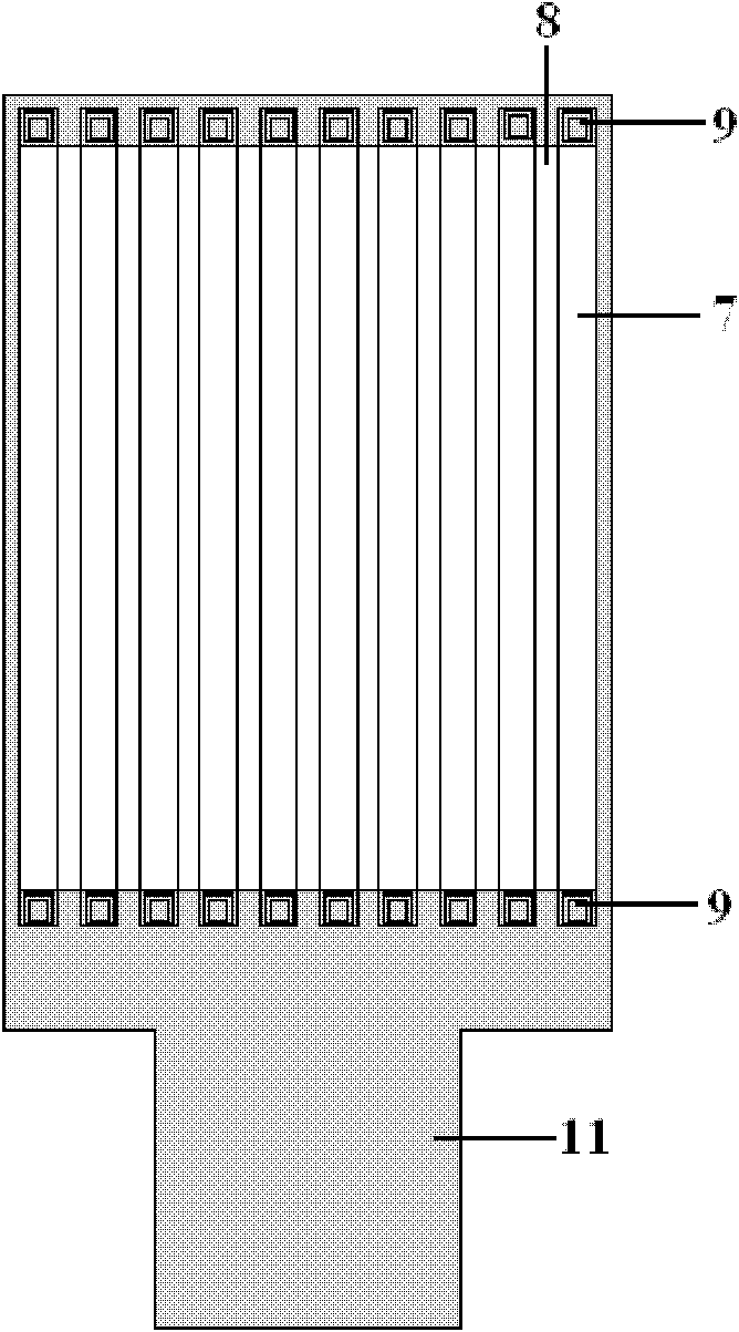
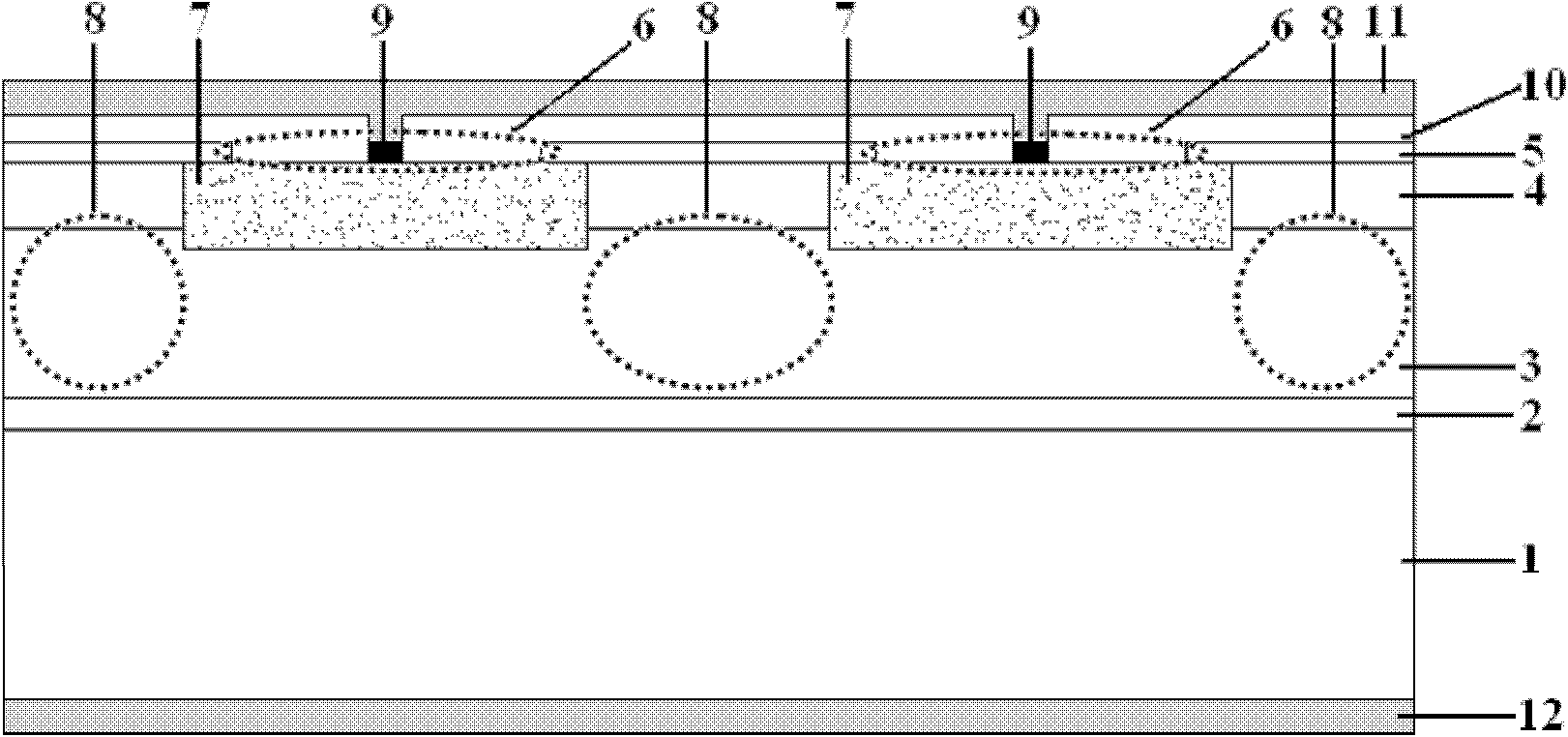
[0026] as attached figure 2 As shown, the epitaxial wafer used in this embodiment adopts metal-organic chemical vapor deposition (MOCVD) technology with a thickness of 300 μm and a carrier concentration > 3×10 18 cm -3 An N-type InP layer 2 with a thickness of 0.5 μm is sequentially grown on the N-type InP substrate 1, and the carrier concentration is >2×10 18 cm -3 ; InGaAs intrinsic absorption layer 3 with a thickness of 2.5 μm and a carrier concentration of 5×10 16 cm -3 ; N-type InP capping layer 4 with a thickness of 1 μm and a carrier concentration of 5×10 16 cm -3 . This embodiment includes a total of 10 sub-pixel diffusion window areas 6, each with a size of 25×500 μm 2 , with a pitch of 15 μm.

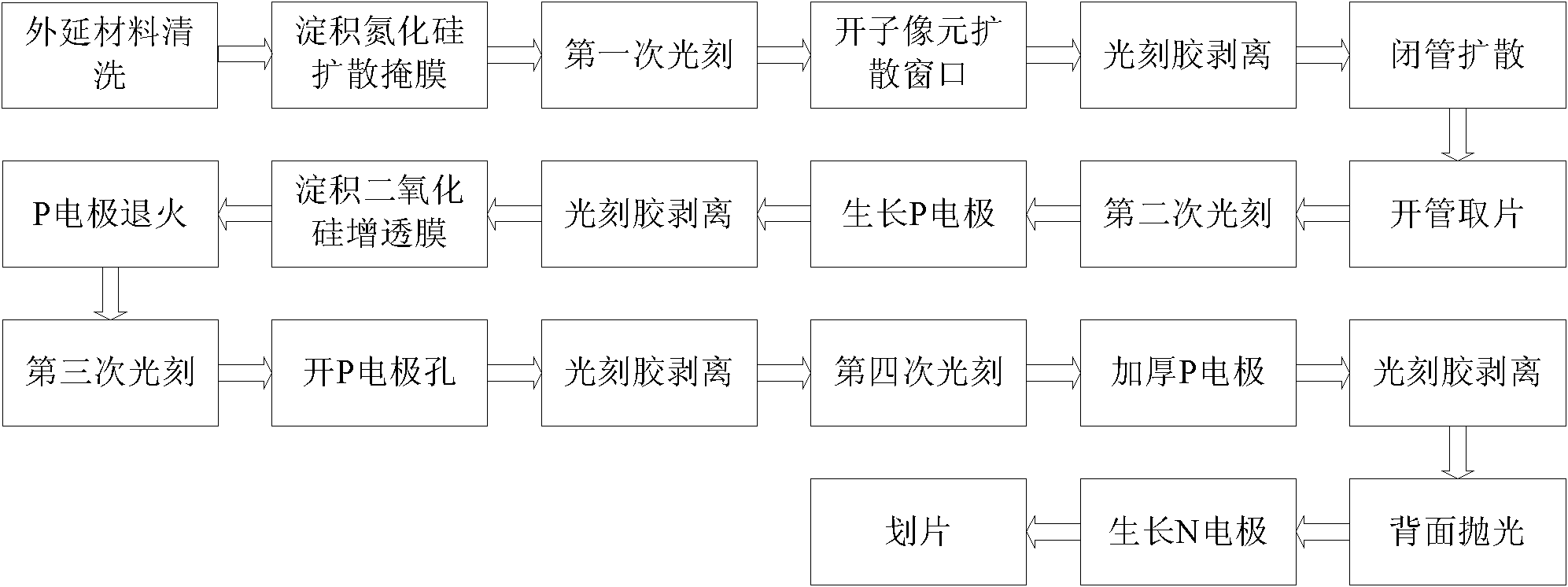
[0027] The specific preparation process steps of the chip of this embodiment are as follows:

[0028] 1) C...


PUM


Abstract

The invention discloses a sub-pixel structured planar InGaAs infrared detector chip which structurally comprises a sub-pixel structured PN node area and a carrier lateral collecting area. The infrared detector chip provided by the invention introduces a sub-pixel structure, utilizes the lateral collection effect of the carrier, and generates a situation that the photoproduction carrier in the carrier lateral collecting area can be effectively absorbed by adjacent sub-pixels; under the condition that quantum efficiency of the detector is not reduced, and a photosensor can respond uniformly; and besides, due to the structure, the diffusion heat damage is effectively reduced with a reduced diffusion area, the surface recombination is reduced with the introduction of double-layered passivation technology, the service life of the minority carrier is prolonged, and the dark current of the device is reduced; and due to the structure, as for a linear detector, the blind pixel rate can be effectively reduced, and the extension and cross talk of the photosensor are suppressed. The novel planar device structure can suppress cross talk, and reduce both device blind pixel rate and device dark current.

Description

technical field [0001] The infrared detector chip involved in the present invention specifically refers to a positively illuminated planar indium gallium arsenide (InGaAs) infrared detector chip. Background technique [0002] InGaAs short-wave infrared detectors can work at room temperature and have broad application prospects. At present, PIN InGaAs detectors are mainly divided into two types: planar type and mesa type. Due to the difficulty of passivation on the side of the mesa device, the reliability of the device is reduced and the dark current is large, which limits the improvement of the detection rate of the device to a large extent. As the mainstream structure of InGaAs detectors, planar detectors have the advantages of easy passivation, low dark current, and high reliability, and are very suitable for the field of aerial remote sensing. However, the planar device has the phenomenon of photosensitive element expansion, and it is difficult to suppress the crosstalk...

Claims


Application Information

Patent Timeline
Patent Type & Authority Applications(China)
IPC IPC(8): H01L27/146H01L31/0216
Inventor 邓洪海唐恒敬李淘李雪魏鹏朱耀明王云姬杨波龚海梅
Owner 无锡中科德芯感知科技有限公司
Why Eureka
Try Eureka