Charge storage unit and image sensor pixel circuit

A pixel circuit and charge storage technology, applied in static memory, digital memory information, circuits, etc., can solve problems such as data errors, charge leakage, and inability to save images for a long time, and achieve the effect of fast read and write speed and low power consumption

Inactive Publication Date: 2012-07-04
SHANGHAI ADVANCED RES INST CHINESE ACADEMY OF SCI
View PDF6 Cites 1 Cited by
  • Summary
  • Abstract
  • Description
  • Claims
  • Application Information

AI Technical Summary

Problems solved by technology

but with figure 1 The structure shown will have the problem of charge leakage in the capacitor C, and the image cannot be saved for a long time. At the same time, it will be more sensitive to external interference, especially in the case of irradiation, the data is prone to errors

Method used


Image

  • Charge storage unit and image sensor pixel circuit
  • Charge storage unit and image sensor pixel circuit
  • Charge storage unit and image sensor pixel circuit

Examples


Embodiment Construction

[0021] The specific implementation manners of the charge storage unit and the image sensor pixel circuit provided by the present invention will be described in detail below in conjunction with the accompanying drawings.

[0022] Unless otherwise specified, the "connection" and "connection" mentioned in this specific embodiment both refer to electrical connection, which means that the front and rear ports are electrically connected.

[0023] Firstly, the first specific implementation manner of the charge storage unit and the image sensor pixel circuit of the present invention will be introduced with reference to the accompanying drawings.

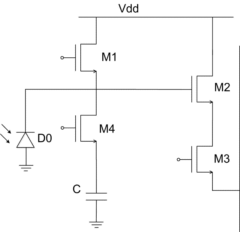
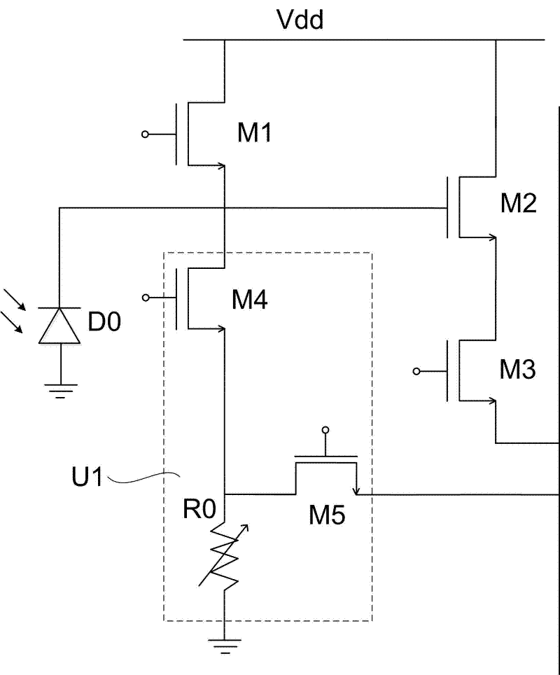
[0024] attached figure 2 Shown is a circuit diagram of the pixel circuit described in this specific embodiment, including a photodiode D0 , a reset transistor M1 , an amplifying transistor M2 , a row selection transistor M3 and a charge storage unit U1 . The input end of the charge storage unit U1 is connected to the cathode D0 of the phot...


PUM


Abstract

The invention provides a charge storage unit, comprising an input end and an output end. The charge storage unit comprises an exposure control transistor, an output transistor and a phase-change resistor, wherein the drain/source electrode of the exposure control transistor is the input end of the charge storage unit, and the drain/source electrode is connected to the first end of the phase-change resistor; the second end of the phase-change circuit is grounded; the drain/source electrode of the output transistor is connected to a co-connecting end of the drain/source electrode of the exposure control transistor with the cathode of a photodiode, the drain/source electrode is the output end of the charge storage unit, and the grid electrode is connected to an output control signal. The charge storage unit has the advantage that a phase-change resistor can be switched between an amorphous state and a crystal state, therefore, optical signals can be stored and voltage signals can be read through externally supplied driving current at last; furthermore, the state of phase-change material is not changed along external temperature or irradiation, and the phase-change material itself has the advantages of no volatility, low energy consumption and rapid reading and writing speed.

Description

technical field [0001] The present invention relates to the field of semiconductor technology, in particular to a charge storage unit and an image sensor pixel circuit. Background technique [0002] A CMOS image sensor is a semiconductor device manufactured using a CMOS manufacturing process that converts an image's optical signal into an electrical signal for transmission and processing. A CMOS image sensor generally consists of a photosensitive area and a signal processing circuit. At present, the common CMOS image sensor is the active pixel image sensor (APS), which is divided into two categories: three-tube image sensor (3T) and four-tube image sensor (4T). [0003] For the traditional 3T pixel circuit, in order to improve the dynamic range of the sensor, a mode of two long and short exposure times is adopted to collect dark light signals and bright light signals respectively, and finally a larger dynamic range is obtained through back-end signal processing. [0004] a...

Claims


Application Information

Patent Timeline
Patent Type & Authority Applications(China)
IPC IPC(8): H01L27/24H01L27/146G11C19/28
Inventor 汪辉丁毅岭陈杰方娜田犁
Owner SHANGHAI ADVANCED RES INST CHINESE ACADEMY OF SCI
Why Eureka
Try Eureka