Nanowire field effect transistor with split-gate structure

A field effect transistor, split gate technology, applied in semiconductor devices, electrical components, circuits, etc., can solve problems such as performance degradation, achieve performance optimization, improve current switching ratio, and improve the effect of on-state current

Inactive Publication Date: 2012-07-04
PEKING UNIV
View PDF5 Cites 7 Cited by
  • Summary
  • Abstract
  • Description
  • Claims
  • Application Information

AI Technical Summary

Problems solved by technology

Due to the limitation of short channel effect and other limitations of tradi

Method used


Image

  • Nanowire field effect transistor with split-gate structure
  • Nanowire field effect transistor with split-gate structure
  • Nanowire field effect transistor with split-gate structure

Examples


Example Embodiment

[0015] Embodiment 1. Nanowire field effect transistor with split gate structure and its performance test

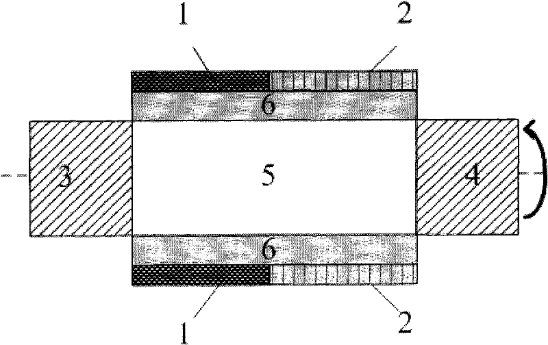
[0016] The structure diagram of the nanowire field effect transistor of the split gate structure is as follows figure 1 As shown, the transistor is composed of split gate electrodes 1 and 2, a source region 3, a drain region 4, a channel region 5 and a gate dielectric layer 6; wherein, the channel region 5 is columnar and is located in the center of the nanowire field effect transistor The gate dielectric layer 6 coaxially and fully encloses the channel region 5; the split gate electrodes 1 and 2 are located outside the gate dielectric layer 6 and coaxially and fully enclose the channel region 5, and the materials constituting the split gate electrodes 1 and 2 are two different The split gate electrodes 1 and 2 are externally connected with the same electrical bias; the source region 3 and the drain region 4 are located on both sides of the channel region 5.

[0017] The diame...


PUM

PropertyMeasurementUnit
Work functionaaaaaaaaaa
Diameteraaaaaaaaaa
Thicknessaaaaaaaaaa

Abstract

The invention discloses a nanowire field effect transistor with a split-gate structure. The transistor is formed by a split-gate electrode, a source region, a drain region, a channel region and a gate dielectric layer, wherein the channel region is columnar and is positioned in the center of the nanowire field effect transistor, and a material forming the channel region is a semiconductor material; the gate dielectric layer totally encircles the channel region coaxially; the split-gate electrode is positioned outside the gate dielectric layer and totally encircles the gate dielectric layer coaxially, and materials forming the split-gate electrode include two kinds of different materials; and the source region and the drain region are positioned at two sides of the channel region respectively. The introduction of the split-gate electrode structure can effectively improve the on-state current of nanowire transistors in prior arts and improve the current switch ratio and the working speed of devices. Simultaneously, the transistor is less affected by threshold voltage shift and drain induced barrier lowering effect resulted from short channel effect, and the performance of size reduction is more excellent.

Description

technical field [0001] The invention relates to a semiconductor integrated circuit device, in particular to a nanowire field effect transistor with a split gate structure. Background technique [0002] The integrated circuit industry's pursuit of higher speed, higher integration, and lower power consumption is driving the development of semiconductor technology, and the feature size of semiconductor devices is getting smaller and smaller. Due to the limitation of short channel effect and other limitations of traditional field effect transistors at nanometer size, the performance is degraded. New device structures have been proposed, including silicon-on-insulator, double-gate, triple-gate, and nanowire field-effect transistors. Among them, the nanowire field effect transistor can provide a high current switching ratio, and is less affected by the short channel effect and the leakage-induced barrier lowering effect. On the basis of existing nanowire field effect transistors...

Claims


Application Information

Patent Timeline
IPC IPC(8): H01L29/78H01L29/423H01L29/06
Inventor 周旺张立宁何进
Owner PEKING UNIV
Why Eureka
Try Eureka