Method for forming crystalline silicon film and plasma CVD device

A film-forming method and plasma technology, which are applied in the fields of plasma, semiconductor/solid-state device manufacturing, gaseous chemical plating, etc., can solve the problems of decreased crystallinity of crystalline silicon film, deterioration of film quality, etc., and reduce thermal budget. Effect

Inactive Publication Date: 2012-07-04
TOKYO ELECTRON LTD
View PDF3 Cites 3 Cited by
  • Summary
  • Abstract
  • Description
  • Claims
  • Application Information

AI Technical Summary

Problems solved by technology

However, it is known that when SiH per unit time 4 When the flow rate increases, the crystallinity of the formed crystalline silicon film decreases, and the film quality deteriorates
Therefore, it is difficult to form a crystalline silicon film with excellent film quality in a short period of time by plasma CVD, which has become a bottleneck in mass production of crystalline silicon films on an industrial scale

Method used


Image

  • Method for forming crystalline silicon film and plasma CVD device
  • Method for forming crystalline silicon film and plasma CVD device
  • Method for forming crystalline silicon film and plasma CVD device

Examples


Embodiment Construction

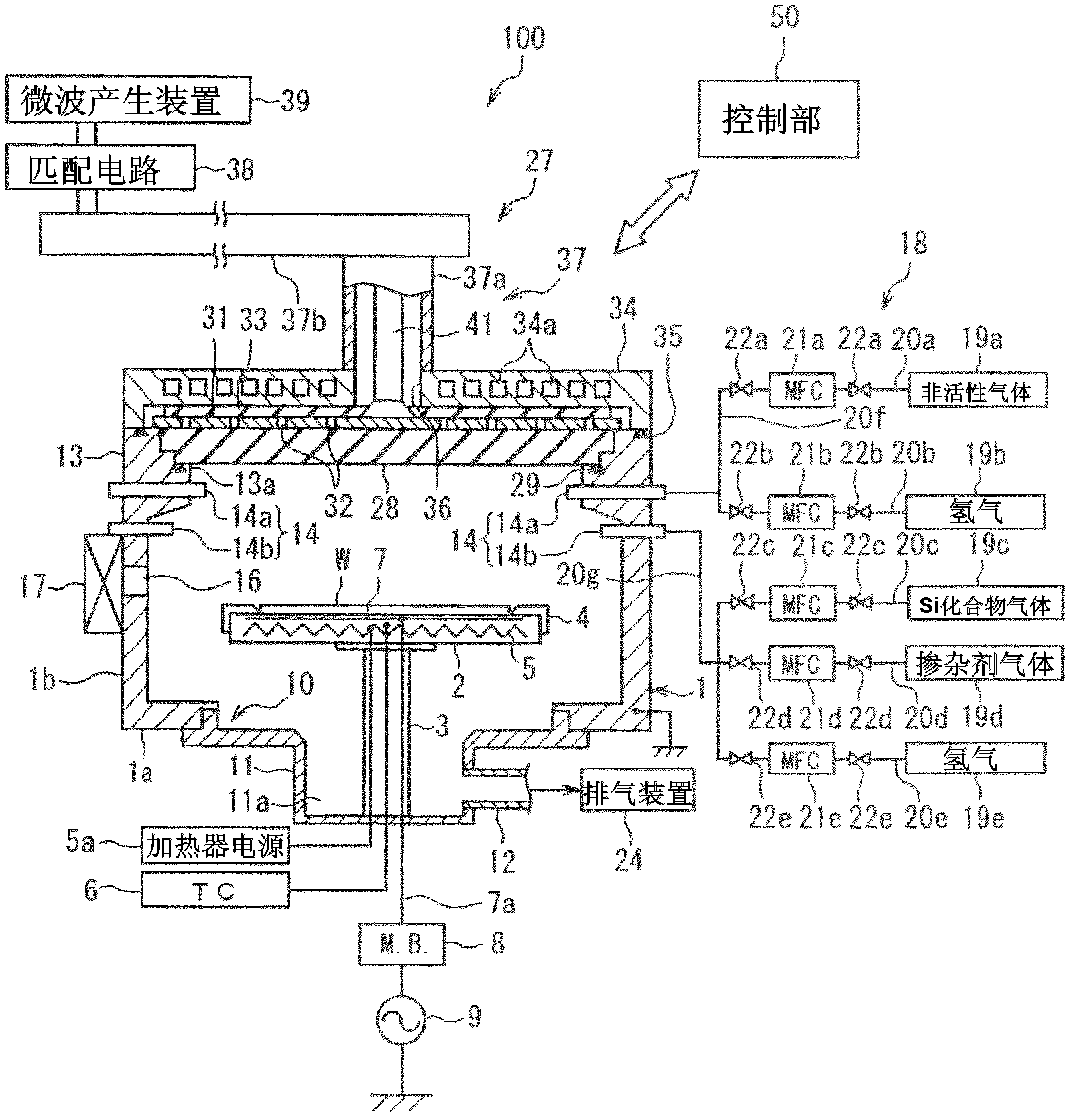
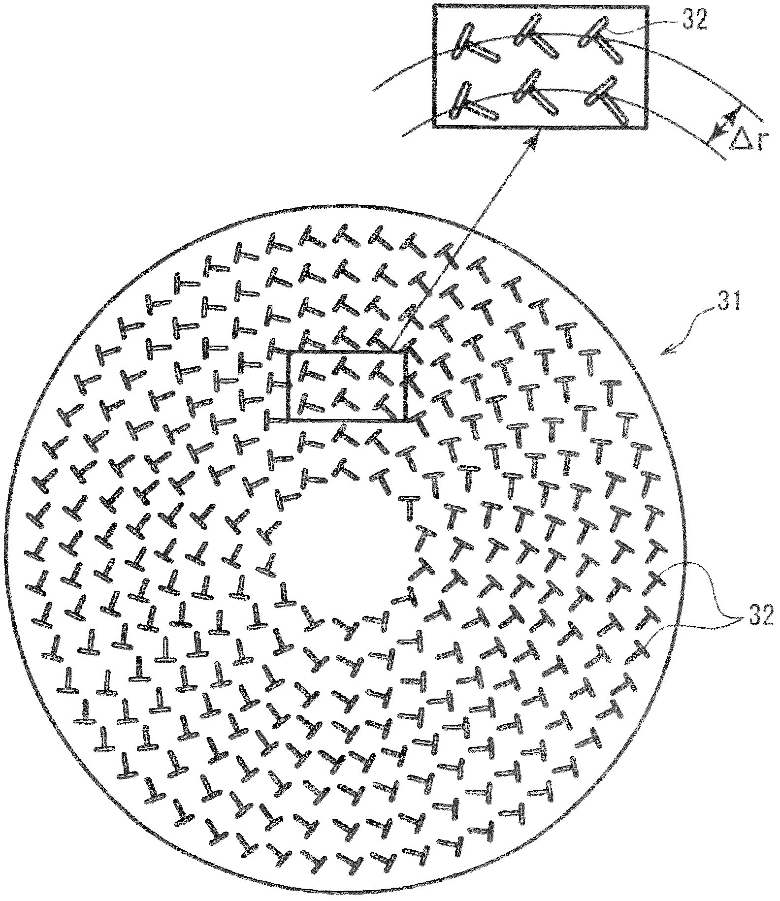
[0044] Hereinafter, embodiments of the present invention will be described in detail with reference to the drawings. figure 1 It is a cross-sectional view schematically showing a schematic configuration of a plasma CVD apparatus 100 that can be used in the method for producing a crystalline silicon film of the present invention.

[0045] The plasma CVD apparatus 100 is configured as an RLSA microwave plasma processing apparatus that introduces microwaves into The plasma is generated inside the processing container, whereby microwave-excited plasma with high density and low electron temperature can be generated. In the plasma CVD apparatus 100, it is possible to use a plasma density of 1×10 10 ~5×10 12 / cm 3 And a plasma with a low electron temperature of 0.7-2eV is used for processing. Accordingly, the plasma CVD apparatus 100 can be applied to a film formation process of forming a polysilicon film which is a crystalline silicon film by plasma CVD in the manufacturing proc...


PUM


Abstract

Provided is a method for forming a high-quality crystalline silicon film at a high film-formation rate by means of plasma CVD. Using a plasma CVD device for introducing microwaves from a planar antenna which has multiple holes, to inside a treatment vessel in order to generate plasma, a film-forming gas including a silicon compound represented by the formula SinH2n+2 (where n is a number of 2 or greater) is excited by microwaves, plasma is generated, and a crystalline silicon film is deposited on the surface of an object to be treated by performing plasma CVD using said plasma.

Description

technical field [0001] The present invention relates to a method for forming a crystalline silicon film and a plasma CVD apparatus. Background technique [0002] Crystalline silicon is a substance that can be doped at a high concentration, and is widely used, for example, in semiconductor devices such as diodes. In the production of the crystalline silicon film, a thermal CVD method and a plasma CVD method using plasma excited by high frequency are used. The thermal CVD method and the plasma CVD method currently do not use monosilane (SiH 4 ) other than gases. [0003] In order to increase the film formation rate in plasma CVD, the SiH 4 It is effective to increase the flow rate per unit time. However, it is known that when SiH per unit time 4 When the flow rate becomes larger, the degree of crystallinity of the formed crystalline silicon film decreases, and the film quality deteriorates. Therefore, it is difficult to form a crystalline silicon film with excellent film...

Claims


Application Information

Patent Timeline
Patent Type & Authority Applications(China)
IPC IPC(8): H01L21/205C23C16/24C23C16/511
CPCH01L21/02532H01L21/0262H01J37/3222H05H1/46C23C16/511C23C16/24H01L21/02573H01J2237/3321H01J37/32192H01L21/02381H01L21/205
Inventor 片山大介本多稔鸿野真之中西敏雄
Owner TOKYO ELECTRON LTD
Why Eureka
Try Eureka