Chip bonding device, chip bonding method and chip bonding quality evaluation equipment

A technology of chip bonding and bonding parts, which is applied in the field of chip bonding quality evaluation equipment, can solve the problems of lengthening the manufacturing process and hindering cost reduction, and achieve the effects of reducing gaps, ensuring bonding strength, and ensuring mechanical strength

Inactive Publication Date: 2012-07-11
HITACHI HIGH TECH INSTR CO LTD
View PDF3 Cites 4 Cited by
  • Summary
  • Abstract
  • Description
  • Claims
  • Application Information

AI Technical Summary

Problems solved by technology

However, batch processing is necessary for evacuation, and after cooling, flux residues remain and a cleaning process is required, so the manufacturing process becomes longer, which is an important factor hindering cost reduction.

Method used


Image

  • Chip bonding device, chip bonding method and chip bonding quality evaluation equipment
  • Chip bonding device, chip bonding method and chip bonding quality evaluation equipment
  • Chip bonding device, chip bonding method and chip bonding quality evaluation equipment

Examples


Embodiment 1

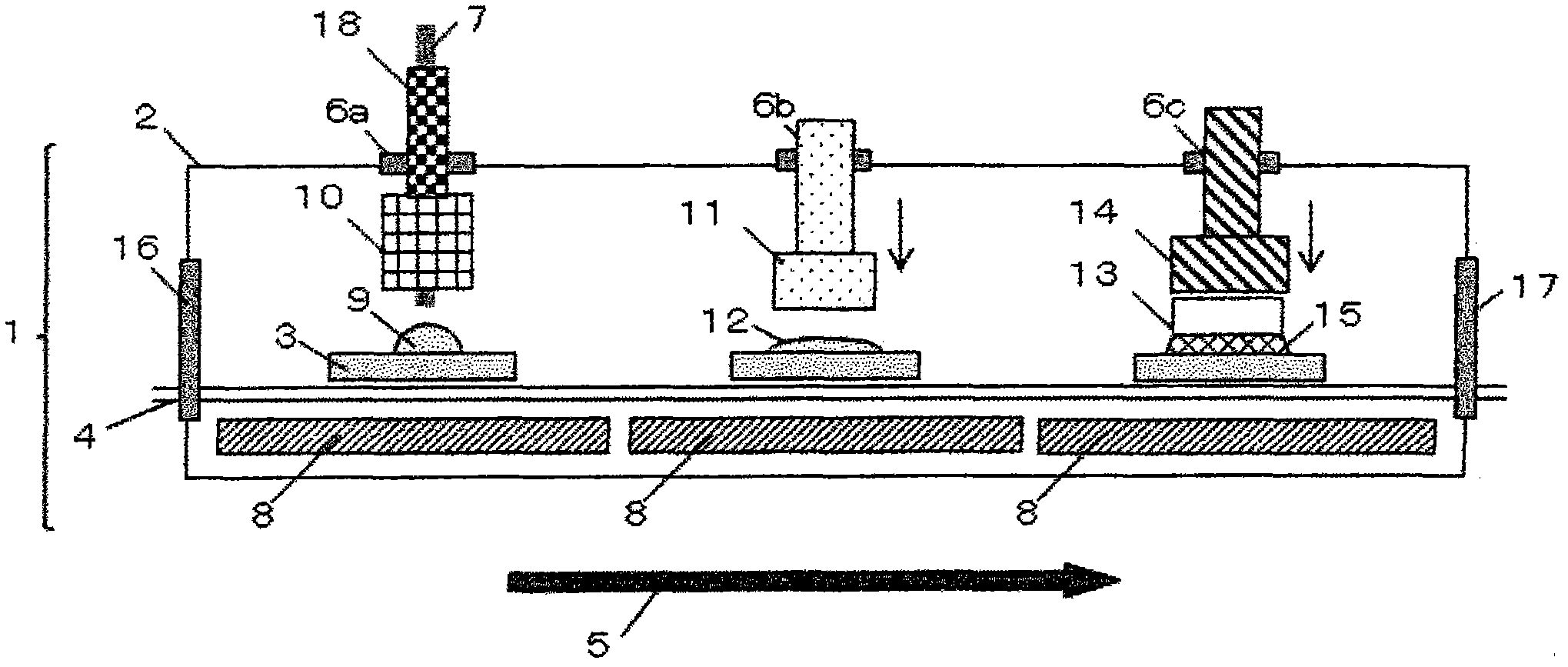
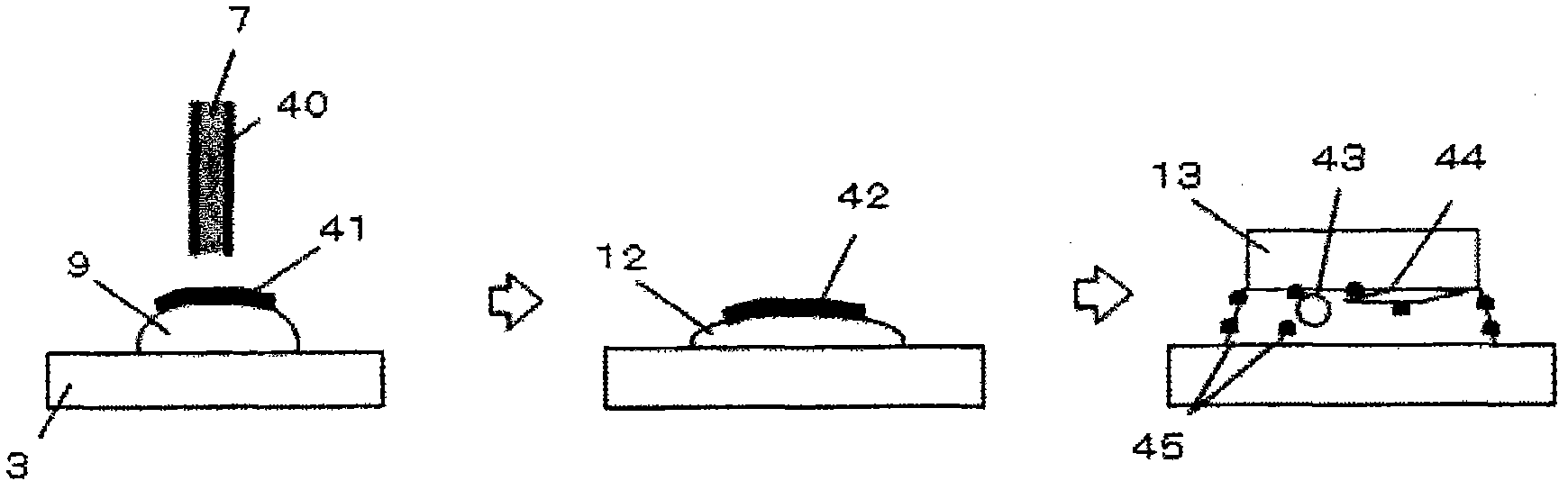
[0040] figure 1 It is an enlarged view of the main part of the die bonder with the solder surface cleaning unit of the present invention. This die bonder 1 is a device that is covered by a case 2 in order to block the outside air, has a guide rail 4 that intermittently moves a plurality of lead frames or substrates 3 as parts to be bonded, and runs along the lead frames or substrates 3. There are three opening windows 6a, 6b, 6c at predetermined positions on the casing (chamber) 2 in the moving direction 5. If it is described in terms of the chip bonding process, the first step is a solder supply part, which supplies long solder wires 7 to the lead frame or the substrate 3 through the opening window 6a. If this process is described in detail, the solder wire 7 sent from the solder supply nozzle 18, after passing through the surface cleaning unit 10, contacts the lead frame or the substrate 3 heated by the heater 8, and the front end of the solder wire 7 melts to wet the lead ...

Embodiment 2

[0059] As Embodiment 2 of this invention, the case where the atmospheric-pressure plasma processing method is used for the solder surface cleaning means is demonstrated. Other than that, it is the same as in Example 1. As the gas for the atmospheric pressure plasma processing, the mixed gas of nitrogen and hydrogen used as the atmospheric gas at the time of die bonding can be used as usual, and a new gas for processing is not required. However, a mixed gas of helium and hydrogen, a mixed gas of argon and hydrogen, or the like may be used in addition. In addition, since the treatment is carried out under atmospheric pressure, there is no need for opening and closing doors at the upper and lower ends of the solder surface cleaning unit 10, and it is possible to reduce the time for vacuum replacement, etc., and continuous treatment is possible, so the productivity is high. The way.

[0060] The plasma jet is arranged so as to collide with the side of the solder line 7 , but if ...

Embodiment 3

[0063] In Embodiment 3 of the present invention, a case where a method of reducing in an electrolytic solution is adopted as the solder surface cleaning means will be described. Other than that, it is the same as in Example 1. In this method, the solder wire 7 is passed through the electrolytic solution, and an electric current is passed through the part immersed in the solution, thereby causing reduction of the oxide film. Thereby, the amount of Sn oxide film on the solder wire can be reduced, and the voids in the die-bonding portion can be reduced, preventing wetting failure, and achieving high quality.


PUM


Abstract

The present invention provides a chip bonding device which can reduce unqualified bonding of gaps and interfaces in bonding parts, a chip bonding method using the same, and chip bonding quality evaluation equipment. Through the chip bonding device, chip bonding quality can be enhanced, and the chip bonding device can utilize soldering tin to bond a semiconductor chip on a lead frame or a substrate. The device is characterized in that the device is provided with a conveying part for conveying the above lead frame or the substrate; a soldering tin supplying part for providing soldering tin for the lead frame or the substrate; a lapping part for lapping and bonding the semiconductor chip to the soldering tin of the lead frame or the substrate; and a surface purification unit for erasing oxidation film of the surface of the soldering tin before the soldering tin is provided to the lead frame or the substrate.

Description

technical field [0001] The present invention relates to a chip bonding device, a chip bonding method, and a chip bonding quality evaluation device. Background technique [0002] In a semiconductor device using a lead frame, generally, a semiconductor chip is mounted on a pad portion of the lead frame, and electrodes of the semiconductor chip and electrodes of the lead frame are electrically connected by wire bonding or the like. Then, the surroundings of the semiconductor chip and the above-mentioned wiring parts such as wire bonding are molded with resin, and the part of the lead frame outside the resin part is cut so as to form a predetermined lead shape, thereby obtaining individual semiconductor devices. [0003] In ordinary semiconductor devices, adhesives are often used to connect the lead frame and the semiconductor chip. In semiconductor devices that use large currents, high power, etc., it is necessary to transfer the heat generated on the semiconductor chip to the ...

Claims


Application Information

Patent Timeline
Patent Type & Authority Applications(China)
IPC IPC(8): B23K3/00B23K3/06H01L21/60
CPCH01L24/743H01L24/75H01L24/27H01L2224/83192
Inventor 秦英惠福田正行市川良雄牛房信之
Owner HITACHI HIGH TECH INSTR CO LTD
Why Eureka
Try Eureka