Resonant-coupling two-way transmission photon crystal waveguide and manufacturing method thereof

A photonic crystal waveguide, bidirectional transmission technology, applied in optical waveguides, light guides, optics, etc., can solve the problems of difficult control of distance parameters between graded optical fibers and photonic crystal devices, the influence of integration, and limitations, and achieve compact structure and high integration. The effect of high degree and simple structure

Inactive Publication Date: 2012-07-11
CHANGCHUN INST OF OPTICS FINE MECHANICS & PHYSICS CHINESE ACAD OF SCI
View PDF4 Cites 5 Cited by
  • Summary
  • Abstract
  • Description
  • Claims
  • Application Information

AI Technical Summary

Problems solved by technology

The evanescent wave method also faces some problems, such as the processing of a specific graded fiber, the difficulty in controlling the distance parameters between the graded fiber used in the coupling process and the photonic crystal device, and the need for a sophisticated external calibration and adjustment system and an external calibration adjustment system The impact on the integration degree and other issues limit the application of the evanescent wave coupling method

Method used


Image

  • Resonant-coupling two-way transmission photon crystal waveguide and manufacturing method thereof
  • Resonant-coupling two-way transmission photon crystal waveguide and manufacturing method thereof
  • Resonant-coupling two-way transmission photon crystal waveguide and manufacturing method thereof

Examples


specific Embodiment approach 1

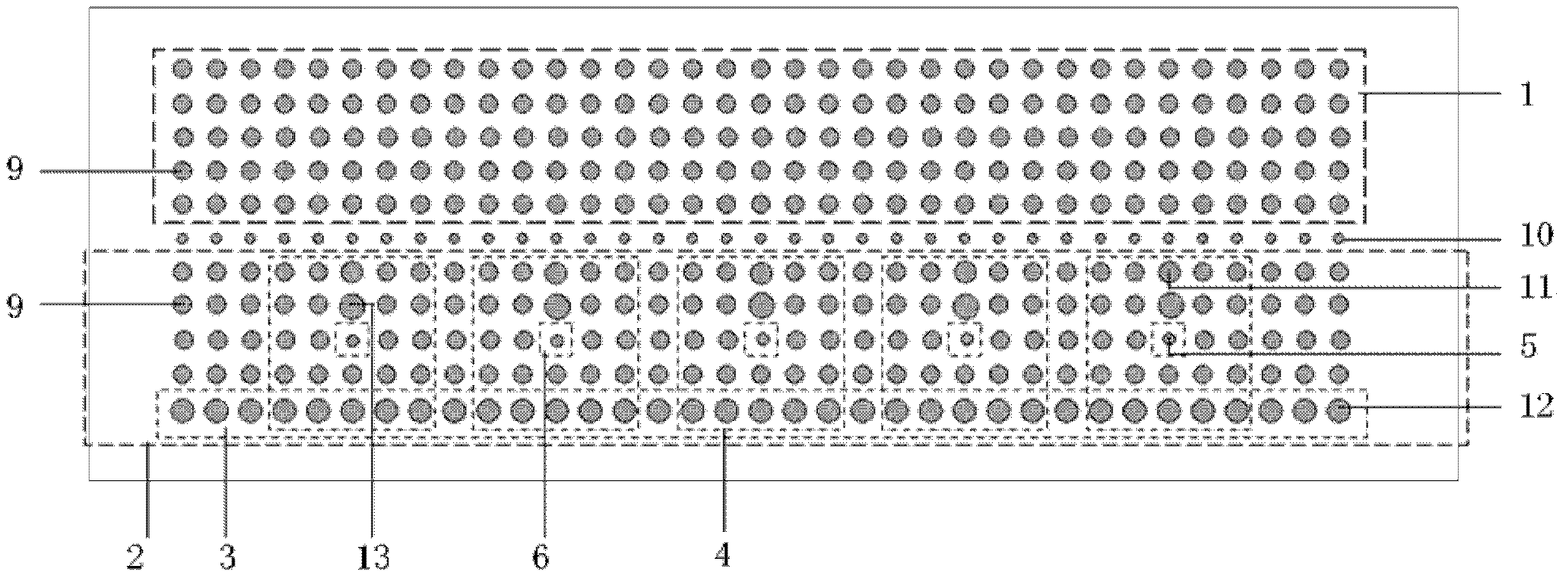
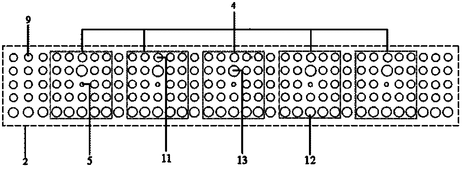
[0024] Specific implementation mode 1. Combination Figure 1 to Figure 5 In this embodiment, the resonantly coupled bidirectional transmission photonic crystal waveguide includes a waveguide layer, a low refractive index buried layer 7 and a substrate silicon layer 8. The waveguide layer is located on the upper part of the low refractive index buried layer 7, and the lower part of the low refractive index buried layer The bottom silicon layer 8 is connected; the waveguide layer includes a first waveguide area 1, a defect area and a second waveguide area 2, the first waveguide area 1 is composed of a plurality of dielectric columns 9 periodically arranged, the first waveguide area 1 and the second waveguide area 2 A row of defective dielectric pillars 10 is distributed at the junction of the waveguide, and the row of defective dielectric pillars 10 constitutes a defect region. A row of coupling dielectric pillars 12 is distributed on the outermost part of the second waveguide re...

specific Embodiment approach 2

[0038] Specific embodiment two, combine Figure 6 to Figure 9 This embodiment is described. This embodiment is a method for manufacturing the resonantly coupled bidirectional transmission photonic crystal waveguide described in Embodiment 1. The method is implemented by the following steps:

[0039] The first step is to prepare the scribing groove required for scribing;

[0040] (A) is 600 μm thick to substrate silicon 101, grows the base of 3 μm thick silicon dioxide buried layer 102 on it (such as Figure 6a shown) for cleaning;

[0041] (B) if Figure 6b As shown, a layer of lanthanum aluminate film 103 is prepared on the silicon dioxide buried layer 102 by a sol-gel method;

[0042] (C) if Figure 6c As shown, a photoresist film 104 with a thickness of 2-3 μm is formed on the lanthanum aluminate film 103;

[0043] (D) putting the completed structure of step (C) into an oven for drying;

[0044] (E) if Figure 6d As shown, the photoresist film 104 is exposed to ultra...


PUM


Abstract

A resonant-coupling two-way transmission photon crystal waveguide and a manufacturing method thereof relate to a micro-structure photonic crystal component in the optical technology field. The invention provides the coupling waveguide and the manufacturing method which can realize high efficient coupling between the photonic crystal waveguide and a traditional optical element or an external light source. According to the invention, a mode that a plurality of photonic-crystal resonant cavities are parallel to each other is used. Through a coupled zone of a waveguide second area, an electromagnetic wave is coupled into a photonic crystal waveguide defect area so as to achieve a purpose of increasing a coupling area. Coupling efficiency is high. Simultaneously, because of the increasing of the coupling area, convenience can be provided for operations, such as prefocusing before the coupling, alignment and the like. Because coupling medium columns are distributed on a position of an upper portion of the photonic-crystal resonant cavity, the coupling efficiency can be further increased, wherein the position corresponds with the position of a point defect. Besides, the whole photonic crystal waveguide is integrated on a same substrate. The external optical element is not needed so that the photonic crystal waveguide structure is compact, a volume is small and an integration level is high.

Description

technical field [0001] The invention relates to a microstructure photonic crystal element in the field of optical technology, in particular to a resonant coupling bidirectional transmission photonic crystal waveguide and a manufacturing method. Background technique [0002] Photonic crystals are artificial microstructures formed by substances with different dielectric constants arranged periodically in space. In recent years, optoelectronic functional devices based on photonic crystal materials have received extensive attention. Photonic crystal optoelectronic devices such as photonic crystal waveguides, filters, optical switches, and couplers have been used The report has laid a good foundation for the realization of large-scale optoelectronic integration and all-optical networks in the future. [0003] Photonic crystals are artificial microstructures formed by periodic arrangements of media with different refractive indices. When electromagnetic waves propagate in them du...

Claims


Application Information

Patent Timeline
Patent Type & Authority Applications(China)
IPC IPC(8): G02B6/122G02B6/13G02B6/138
Inventor 王维彪梁中翥梁静秋周建伟
Owner CHANGCHUN INST OF OPTICS FINE MECHANICS & PHYSICS CHINESE ACAD OF SCI
Why Eureka
Try Eureka