

SONOS (Silicon Oxide Nitride Oxide Silicon) unit transistor with high erasing speed and manufacturing method thereof
A technology of erasing and writing speed and transistors, which is applied in semiconductor/solid-state device manufacturing, electrical components, semiconductor devices, etc., can solve the problem of low thermal electron injection programming efficiency, improve programming efficiency and speed, reduce energy valley scattering probability, The effect of effective mass reduction
- Summary
- Abstract
- Description
- Claims
- Application Information
AI Technical Summary
Problems solved by technology
Method used
Image

Examples
Embodiment Construction
[0026] The present invention will be described in further detail below in conjunction with the accompanying drawings and specific embodiments. The specific embodiments described here are only used to explain the present invention, and are not used to limit the protection scope of the present invention.
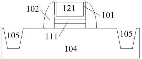
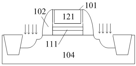
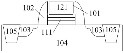
[0027] first reference image 3 and Figure 4 , the SONOS cell transistor of the present invention with a high erasing and writing speed includes as shown in the figure: several pairs of PMOS (not shown in the drawings) and NMOS, and the NMOS includes: a P-type transistor with several pairs of active regions 103 Silicon substrate 104, a channel is formed between each pair of active regions 103 ( image 3 and Figure 4 not shown in); the gate 101 is located above the channel, and there is a silicon oxide-silicon nitride-silicon oxide layer 111 (ONO layer) between the sidewalls 102 of the gate 101, and the silicon oxide- On the silicon nitride-silicon oxide layer 111 is poly...
PUM
 Abstract
Description
Claims
Application Information