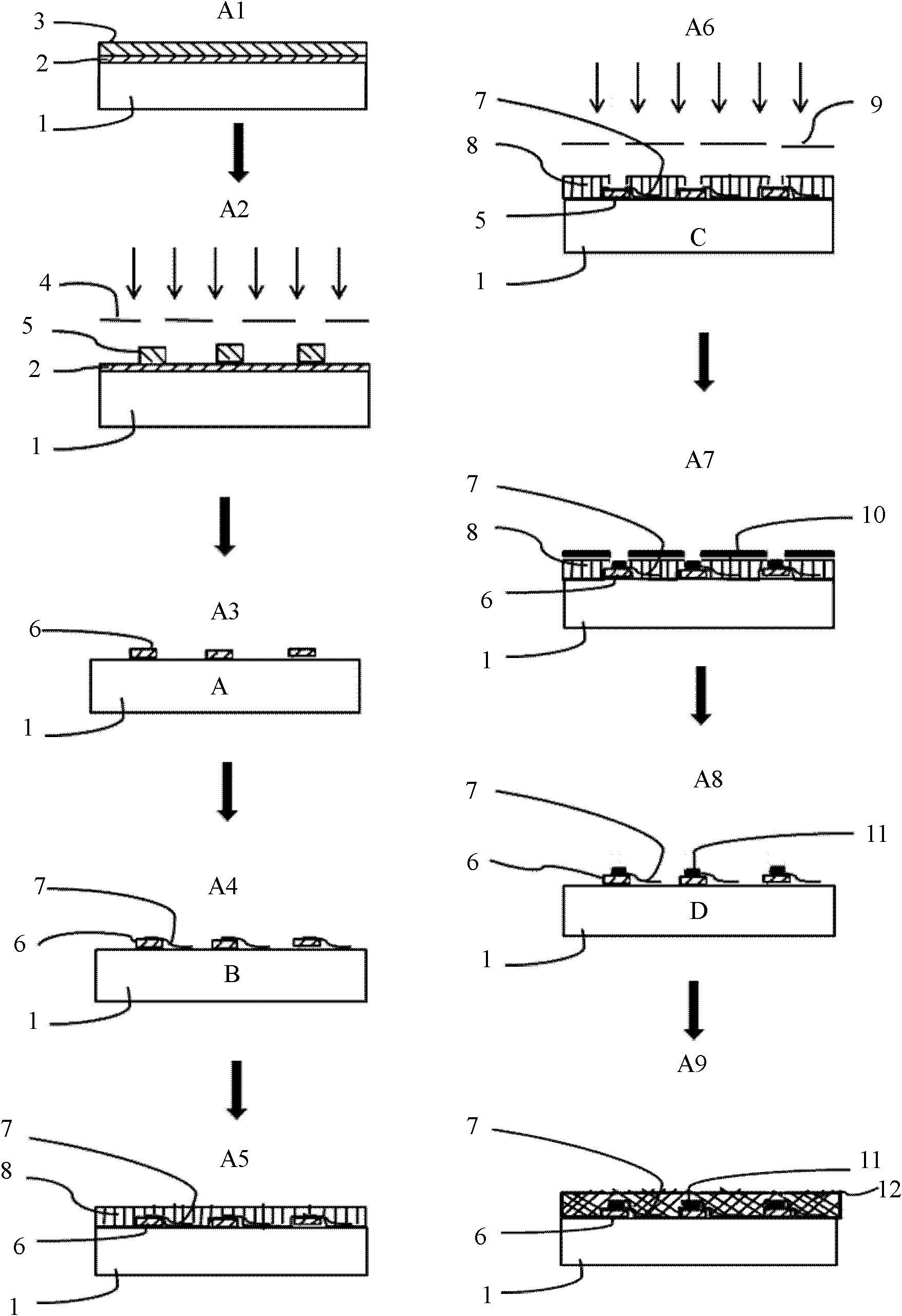
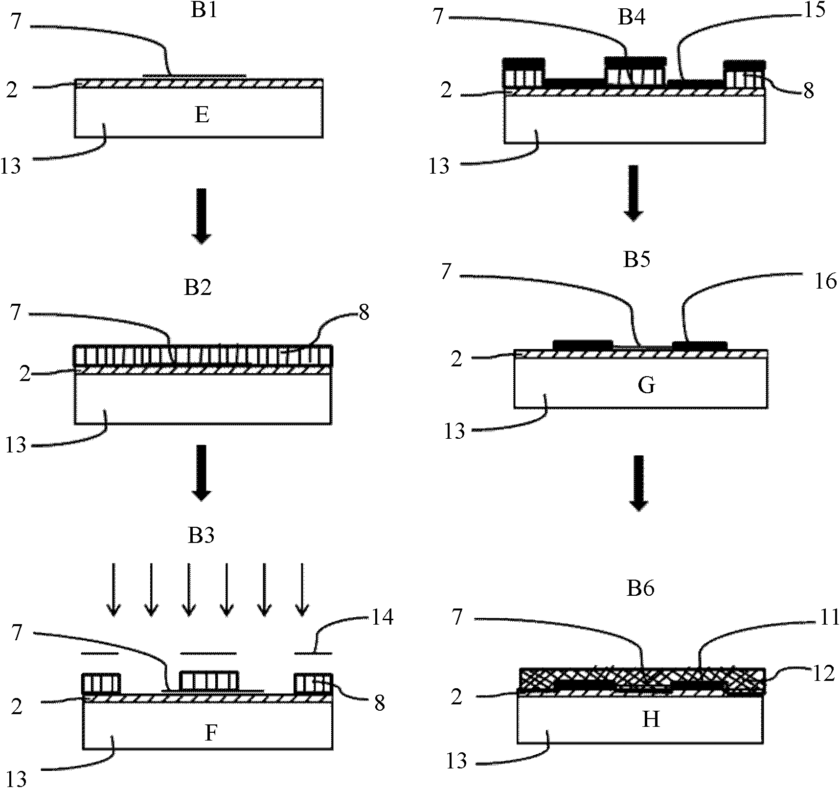
Method for preparing p-CdS nano wire and p-CdS/n-Si nano p-n node through manganese trioxide (MoO3) surface doping
A surface doping, nanowire technology, applied in sustainable manufacturing/processing, final product manufacturing, electrical components, etc. The effect of mass production, high electrical stability, and stable performance
- Summary
- Abstract
- Description
- Claims
- Application Information
AI Technical Summary
Problems solved by technology
Method used
Image

Examples
Embodiment 1
[0036] Weigh 1.0g of CdS powder with a purity higher than 99.9% into Al 2 o 3 In the small porcelain boat, place the small porcelain boat upstream of the dual-temperature zone tube furnace, place an Au-coated silicon wafer 10cm downstream of the carrier gas, the thickness of the Au film is 15nm, and pump the vacuum to 5×10 -3 Below Pa, feed Ar and H at a flow rate of 30 sccm 2 Gas mixture, Ar and H 2 The volume ratio of the mixed gas is 95:5, and the air pressure is maintained at 5×10 3 Pa, the upstream was heated to 850°C and kept for 90 minutes to synthesize intrinsic CdS nanowires.
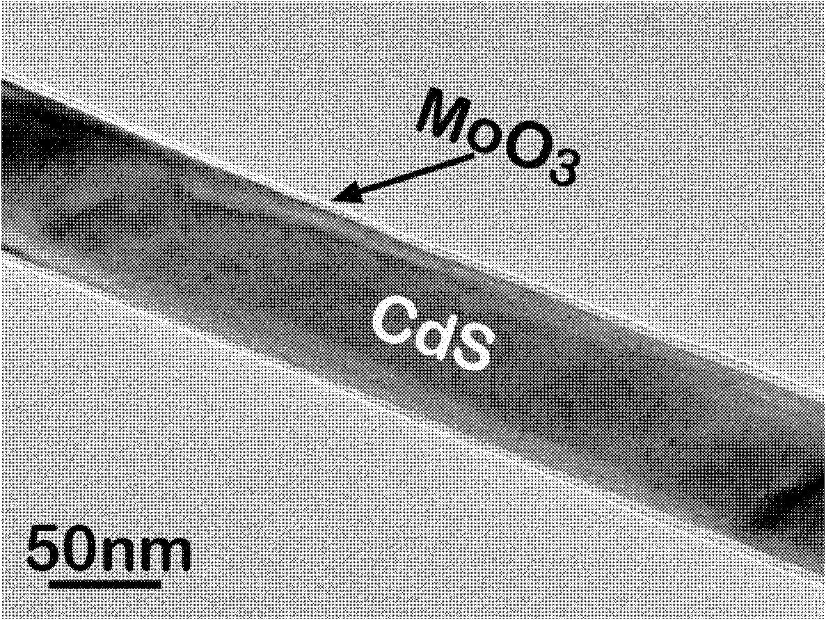
[0037] Directly coat the synthesized intrinsic CdS nanowires with a layer of MoO with a thickness of 5nm by pulsed laser deposition or electron beam thermal evaporation or magnetron sputtering 3 layer.
[0038] Coating the above with MoO 3 The layered CdS nanowires are placed in a rapid annealing furnace for annealing at 150° C. for 15 minutes to obtain p-type CdS nanowires.
[0039] The...
Embodiment 2
[0041] Weigh 1.0g of CdS powder with a purity higher than 99.9% into Al 2 o 3 In the small porcelain boat, place the small porcelain boat upstream of the dual-temperature zone tube furnace, place an Au-coated silicon wafer 10cm downstream of the carrier gas, the thickness of the Au film is 15nm, and pump the vacuum to 5×10 -3 Below Pa, feed Ar and H at a flow rate of 30 sccm 2 Gas mixture, Ar and H 2 The volume ratio of the mixed gas is 95:5, and the air pressure is maintained at 5×10 3 Pa, the upstream was heated to 850°C and kept for 90 minutes to synthesize intrinsic CdS nanowires.
[0042] Use pulsed laser deposition method or electron beam thermal evaporation method or magnetron sputtering method to directly coat the synthesized intrinsic CdS nanowire with a layer of MoO with a thickness of 40nm 3 layer.
[0043] Coating the above with MoO 3 The layered CdS nanowires are placed in a rapid annealing furnace for annealing at 200° C. for 15 minutes to obtain p-type CdS...
Embodiment 3
[0046] Weigh 1.0g of CdS powder with a purity higher than 99.9% into Al 2 o 3 In the small porcelain boat, place the small porcelain boat upstream of the dual-temperature zone tube furnace, place an Au-coated silicon wafer 10cm downstream of the carrier gas, the thickness of the Au film is 15nm, and pump the vacuum to 5×10 -3 Below Pa, feed Ar and H at a flow rate of 30 sccm 2 Gas mixture, Ar and H 2 The volume ratio of the mixed gas is 95:5, and the air pressure is maintained at 5×10 3 Pa, the upstream was heated to 850°C and kept for 90 minutes to synthesize intrinsic CdS nanowires.
[0047] Directly wrap a layer of MoO with a thickness of 80nm on the synthesized intrinsic CdS nanowires by pulsed laser deposition method or electron beam thermal evaporation method or magnetron sputtering method 3 layer.
[0048] coated with MoO 3 The layered CdS nanowires are placed in a rapid annealing furnace for annealing at 200° C. for 15 minutes to obtain p-type CdS nanowires.
[...
PUM
| Property | Measurement | Unit |
|---|---|---|
| Thickness | aaaaa | aaaaa |
| Thickness | aaaaa | aaaaa |
| Thickness | aaaaa | aaaaa |
Abstract
Description
Claims
Application Information
 - Generate Ideas
- Intellectual Property
- Life Sciences
- Materials
- Tech Scout
- Unparalleled Data Quality
- Higher Quality Content
- 60% Fewer Hallucinations
Browse by: Latest US Patents, China's latest patents, Technical Efficacy Thesaurus, Application Domain, Technology Topic, Popular Technical Reports.
© 2025 PatSnap. All rights reserved.Legal|Privacy policy|Modern Slavery Act Transparency Statement|Sitemap|About US| Contact US: help@patsnap.com