Copper line-clad aluminum silicon carbide ceramic substrate applicable to radiation of high-power LED

A technology of aluminum silicon carbide and ceramic substrates, which is applied in the direction of circuits, electrical components, semiconductor devices, etc., can solve the problems of unsuitable aluminum nitride substrates, fragmentation, insufficient strength of anodized oxide layers, etc., and achieve good thermal stability, Simple preparation process and high thermal conductivity

Inactive Publication Date: 2012-07-11
CHINA JILIANG UNIV
View PDF3 Cites 22 Cited by
  • Summary
  • Abstract
  • Description
  • Claims
  • Application Information

AI Technical Summary

Problems solved by technology

[0003] The LED chip substrate is mainly used as a medium for heat export between the LED chip and the system circuit board. The traditional aluminum substrate is mostly used, but the heat dissipation effect is not ideal.
At present, the LED chip substrates on the market are mainly ceramic substrates, including silicon substrates, silicon carbide substrates, anodized aluminum substrates or aluminum nitride substrates. The semiconductor characteristics of silicon and silicon carbide substrate materials make them unavailable at this stage. The anodized aluminum substrate is easily broken due to the insufficient strength of the anodized oxide layer to cause conduction; at this stage, the more mature and generally accepted one is aluminum nitride as the heat dissipation substrate; however, currently limited by nitrogen The aluminum nitride substrate is not suitable for the traditional thick film process (the material must be subjected to an atmospheric heat treatment at 850°C after printing with silver glue, which causes material reliability problems), so there are still many problems with the aluminum nitride substrate
The present invention intends to provide a copper-clad circuit aluminum silicon carbide ceramic substrate for heat dissipation of high-power LED and its preparation method to solve the problem of heat dissipation and stability of high-power LED

Method used


Image

  • Copper line-clad aluminum silicon carbide ceramic substrate applicable to radiation of high-power LED
  • Copper line-clad aluminum silicon carbide ceramic substrate applicable to radiation of high-power LED
  • Copper line-clad aluminum silicon carbide ceramic substrate applicable to radiation of high-power LED

Examples


Embodiment 1

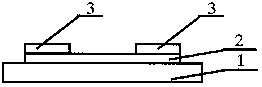
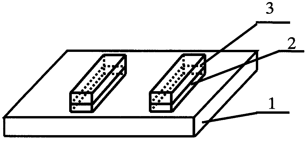
[0025] Implementation example 1: such as figure 1 and figure 2 As shown, a copper-clad circuit aluminum silicon carbide ceramic substrate for high-power LED heat dissipation is characterized in that: it is composed of an aluminum silicon carbide layer (1), a copper aluminum oxide layer (2) and a copper circuit (3); Copper-aluminum oxide layer (2) is on the layer (1), and copper wiring (3) is on the copper-aluminum oxide layer (2); the separation distance between the copper wiring (2) is 1 mm; the width of the copper wiring (2) is 1000 microns, and the height of the copper line (2) is 2 mm.

[0026] A copper-clad circuit aluminum silicon carbide ceramic substrate for high-power LED heat dissipation, comprising the following preparation steps: ① Weighing reagent (SiO 2 , coke and flux), fully mix these components;

[0027] ②Put the above mixture in a high temperature furnace for calcination, the calcination temperature is 1800°C, the rate of temperature increase is 50°C / hour...

Embodiment 2

[0033] Implementation example 2: such as figure 1 and figure 2 As shown, a copper-clad circuit aluminum silicon carbide ceramic substrate for high-power LED heat dissipation is characterized in that: it is composed of an aluminum silicon carbide layer (1), a copper aluminum oxide layer (2) and a copper circuit (3); The copper aluminum oxide layer (2) is on the layer (1), and the copper wiring (3) is on the copper aluminum oxide layer (2); the separation distance range between the copper wiring (2) is 1 mm; the copper wiring (2) The width is in the range of 500 microns, and the height of the copper lines (2) is in the range of 1 mm.

[0034]A copper-clad circuit aluminum silicon carbide ceramic substrate for high-power LED heat dissipation, comprising the following preparation steps: ① Weighing reagent (SiO 2 , coke and flux), fully mix these components;

[0035] ②Put the above mixture in a high-temperature furnace for calcination, the calcination temperature is 2000°C, the...


PUM

PropertyMeasurementUnit
thicknessaaaaaaaaaa
thicknessaaaaaaaaaa
thicknessaaaaaaaaaa

Abstract

A copper line-clad aluminum silicon carbide ceramic substrate applicable to radiation of a high-power LED is characterized by consisting of an aluminum silicon carbide layer (1), a copper and aluminum oxide layer (2) and copper lines (3), wherein the copper and aluminum oxide layer (2) is arranged on the alumina layer (1); the copper lines (3) are arranged on the copper and aluminum oxide layer (2); the distance between the copper lines (2) is 0.1-1mm; the widths of the copper lines (2) are 200-1000 microns; the heights of the copper lines (2) are 0.01-2mm; the copper line-clad aluminum silicon carbide ceramic substrate is manufactured by the following steps: weighing SiO2, coke and a fluxing agent, and preparing the raw materials into porous silicon carbide; heating an aluminum block and melting the aluminum block into liquid aluminum, mixing the liquid aluminum with the porous silicon carbide in a certain ratio, and preparing the mixture into aluminum silicon carbide powder and a high-thermal conductivity aluminum silicon carbide substrate; cladding copper on the aluminum silicon carbide substrate, heating at a high temperature to form an eutectic melt, and forming an aluminum silicon carbide ceramic substrate layer, the copper and aluminum oxide layer and a copper layer from the bottom up; and etching conductive copper lines. The ceramic substrate has a good application prospect in the aspect of the radiation of the high-power LED.

Description

technical field [0001] The invention belongs to the technical field of ceramic heat dissipation materials. Specifically, the invention relates to a copper-clad circuit aluminum silicon carbide ceramic substrate for high-power LED heat dissipation and a preparation method thereof. Background technique [0002] LED products have the advantages of energy saving, power saving, high efficiency, fast response time, long life cycle, and environmental protection benefits, and are one of the most eye-catching industries in recent years. Usually about 15% of the input power of high-power LED products can be converted into light, and the remaining 85% of the electrical energy is converted into heat energy. Excessively high LED p-n junction temperature will lead to LED luminous efficiency attenuation. Therefore, if the heat generated when the LED emits light cannot be dissipated in time, the junction temperature of the LED will be too high, which will affect the product life cycle, lumi...

Claims


Application Information

Patent Timeline
Patent Type & Authority Applications(China)
IPC IPC(8): H01L33/64H01L33/62
Inventor 沈常宇金尚忠李萍钟川褚金雷邹新牟晟
Owner CHINA JILIANG UNIV
Why Eureka
Try Eureka