Thin-film transistor, manufacturing method therefor, and liquid-crystal display device

A thin-film transistor and polysilicon technology, applied in transistors, semiconductor/solid-state device manufacturing, semiconductor devices, etc., can solve the problems of low charge mobility in the channel region and difficult to use, and achieve fast migration speed, large on-current, and low The effect of power consumption

Inactive Publication Date: 2012-07-11
V TECH CO LTD
View PDF10 Cites 10 Cited by
  • Summary
  • Abstract
  • Description
  • Claims
  • Application Information

AI Technical Summary

Problems solved by technology

Recently, someone has proposed a liquid crystal display device in which a driving circuit is formed on a peripheral portion of a substrate forming a pixel portion. Transistors constituting the peripheral drive circuit required for rewriting, the charge mobility of the channel region is too small, making it difficult to use

Method used


Image

  • Thin-film transistor, manufacturing method therefor, and liquid-crystal display device
  • Thin-film transistor, manufacturing method therefor, and liquid-crystal display device
  • Thin-film transistor, manufacturing method therefor, and liquid-crystal display device

Examples


Embodiment Construction

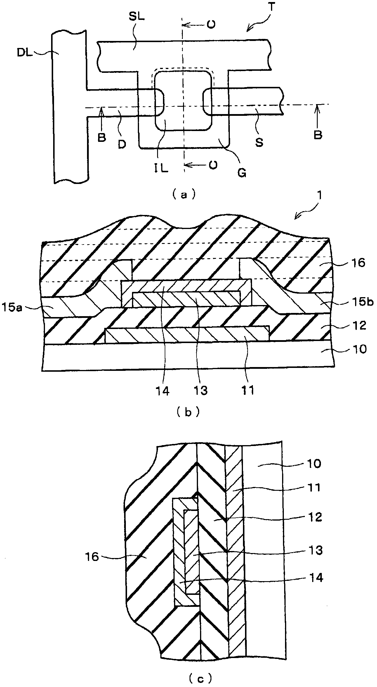
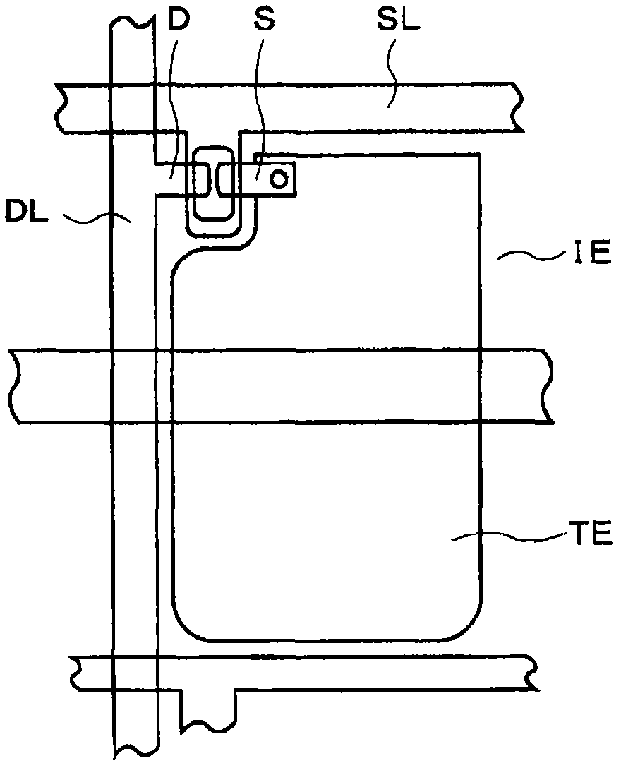
[0025] Hereinafter, embodiments of the present invention will be described in detail with reference to the drawings. figure 1 represents a thin film transistor according to an embodiment of the present invention, figure 2 It is a plan view showing one pixel of the display unit of the liquid crystal display device. In a liquid crystal display device, a display portion and a peripheral circuit for driving in a peripheral portion of the display portion are arranged, and in the display portion, as figure 2 As shown, a plurality of scanning lines SL and a plurality of signal lines DL are formed orthogonally, and one pixel is formed in a unit area surrounded by the scanning lines SL and signal lines DL. In each pixel, a transparent electrode TE made of ITO (Indium Tin Oxide) and a switching transistor T are formed. The gate electrode of the transistor T is connected to the scanning line SL, the drain of the transistor T is connected to the signal line DL, and the source is conne...


PUM


Abstract

Provided is a thin-film transistor comprising a low-temperature polysilicon transistor having a low off-current, excellent potential-holding characteristics, low power usage, and a high operating speed. Also provided are a liquid-crystal display device using said thin-film transistor and a method for manufacturing the thin-film transistor. The provided thin-film transistor uses an inversely staggered structure with a gate electrode, a gate insulation film, a channel region, and source/drain electrodes formed on top of a glass substrate. The channel region comprises a polysilicon film and an a-Si:H film that covers the top and sides of the polysilicon

Description

technical field [0001] The present invention relates to a thin film transistor having an inverted staggered structure, and more particularly to a thin film transistor suitable for a pixel transistor in a display portion of a liquid crystal display device, a method for manufacturing the same, and a liquid crystal display device. Background technique [0002] As an inverted staggered thin film transistor, there is an amorphous silicon transistor in which a gate electrode is formed on an insulating substrate using a metal layer such as Cr or Al, and then a SiN film is formed as a gate insulating film, for example, on a substrate including the gate electrode. A hydrogenated amorphous silicon (hereinafter referred to as "a-Si:H") film is then formed on the entire surface. The amorphous silicon transistor is further formed on the a-Si:H film such as n + Si film, a-Si:H film and n + Si film island pattern, and then use the metal layer to form the source / drain electrode, use the s...

Claims


Application Information

Patent Timeline
Patent Type & Authority Applications(China)
IPC IPC(8): H01L29/786G02F1/1368H01L21/20H01L21/336
CPCH01L29/78696H01L21/02532H01L21/02678H01L29/78678H01L29/66765H01L29/04H01L29/78669H01L29/78609H01L21/2026
Inventor 滨野邦幸
Owner V TECH CO LTD
Why Eureka
Try Eureka