Metal interconnection structure of integrated circuit and preparation method for metal interconnection structure

A metal interconnection structure, integrated circuit technology, applied in the direction of circuits, electrical components, electrical solid devices, etc., can solve the problems of reducing the growth rate of holes, increasing the resistance of interconnection lines, and increasing the resistivity, so as to achieve strong anti-electricity Effect of migration ability, low sheet resistance, thermal stability and chemical stability improvement

Inactive Publication Date: 2012-07-18
PEKING UNIV
View PDF4 Cites 12 Cited by
  • Summary
  • Abstract
  • Description
  • Claims
  • Application Information

AI Technical Summary

Problems solved by technology

Although these covering layers can effectively improve the reliability of the metal interconnection, they will increase the resistance of the interconnection.
In addition, Chai et al. can effectively reduce the growth rate of holes by replacing copper with Cu / CNT composite materials. The growth rate of holes in Cu / CNT composite materials is about a quarter of that of pure copper materials, but the same problem is resistance. The rate is 15% higher than the resistivity of pure copper

Method used


Image

  • Metal interconnection structure of integrated circuit and preparation method for metal interconnection structure
  • Metal interconnection structure of integrated circuit and preparation method for metal interconnection structure
  • Metal interconnection structure of integrated circuit and preparation method for metal interconnection structure

Examples


specific Embodiment

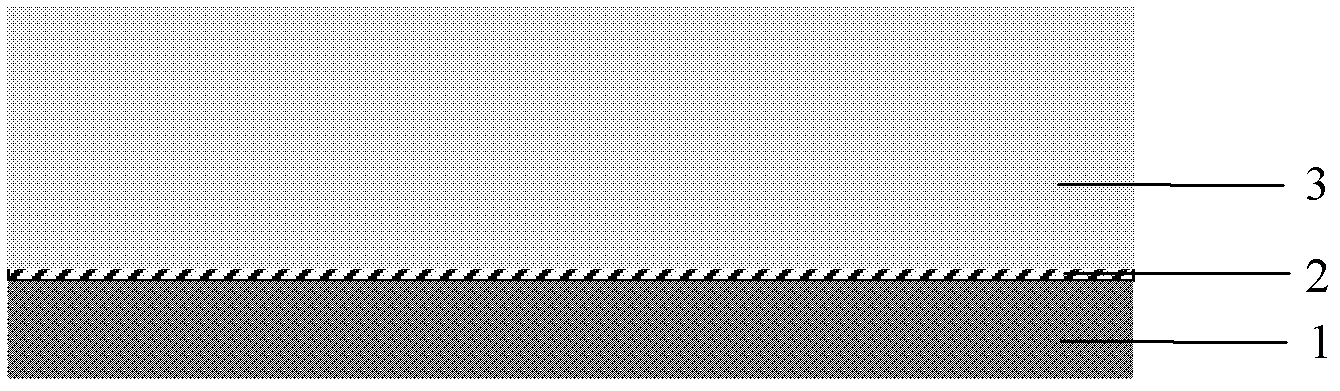
[0020] (1) Preparation of the lower layer copper interconnection 1: the lower layer copper interconnection 1 is prepared by a damascene process, and its surface is chemically mechanically polished and covered with a NiWP layer, such as figure 1 shown.

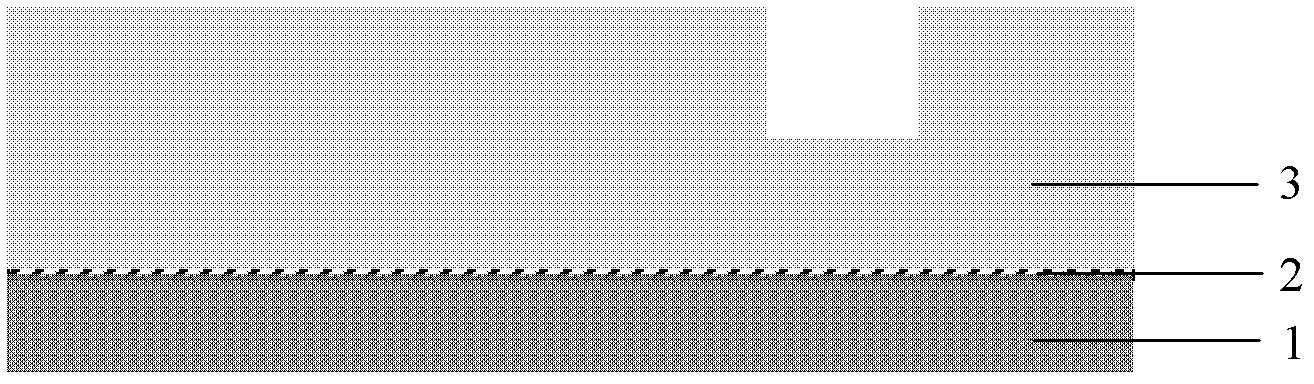
[0021] (2) Depositing a silicon dioxide dielectric layer 3 with a thickness of 1 μm on the lower copper interconnection structure by PECVD, such as figure 2 shown.

[0022] (3) Reactive ion etching (RIE) is used to etch the through hole connecting the lower copper interconnection 1 and the groove of the upper copper interconnection 5 in the silicon dioxide dielectric layer 3 (dual damascene process), Such as image 3 , 4 shown.

[0023] (4) Deposit a layer of 5nm thick TaN as a diffusion barrier layer 4 on the bottom and sidewalls of the vias and trenches by atomic layer deposition, and then use CuCl on it 2 as a reactant, H 2 A 5nm thick copper seed crystal layer was deposited by atomic layer deposition as a reducing a...


PUM


Abstract

The invention discloses a metal interconnection structure of an integrated circuit and a preparation method for the metal interconnection structure. A graphene covering layer is coated on the upper surfaces of upper layer metal interconnection lines of the metal interconnection structure of the integrated circuit by utilizing the proper unique molecular structure and the electrology characteristic of graphene. As the electromigration-resistance current density of the graphene can reach 109A/cm<2>, once when small cavities appear in metal conductors due to electromigration, current can be possibly conducted through the graphene coated on the surfaces of the metal conductors, and thereby, the growth rate of the cavities in the metal interconnection lines is effectively lowered, the electromigration resistance of the metal interconnection lines is increased, and the service lives of the metal interconnection lines are prolonged. Meanwhile, the graphene coated on the surfaces of the metal interconnection lines is also capable of effectively stopping the growth of crystal whiskers, and thereby, the short circuit risk caused by the growth of the crystal whiskers is lowered. Moreover, the graphene covering layer is capable of effectively isolating the metal conductors from contacting with the air so as to retard or eliminate the oxidation of the surfaces of the metal interconnection lines, and thereby, the reliability of the interconnection lines of the integrated circuit is improved.

Description

technical field [0001] The invention relates to nano-processing technology, in particular to an integrated circuit metal interconnection structure and a preparation method thereof. Background technique [0002] With the continuous scaling down of the size of integrated circuit devices and the continuous improvement of circuit integration, the performance of metal interconnection lines in integrated circuits has become one of the key factors affecting the reliability of integrated circuits. Electromigration is the main cause of performance degradation of metal interconnects. The so-called electromigration is the phenomenon of mass transport in metal conductors when the current density reaches a certain value, that is, when the current density is high, the electron density passing through the metal interconnection line is high, and this "electron wind" will A large force opposite to the direction of the original electric field force is applied to the positively charged metal ...

Claims


Application Information

Patent Timeline
Patent Type & Authority Applications(China)
IPC IPC(8): H01L23/532H01L21/768
Inventor 魏芹芹尹金泽曹宇崔晓锐魏子钧赵华波傅云义黄如张兴
Owner PEKING UNIV
Why Eureka
Try Eureka