Multi-porous channel current equalizing-based transient voltage suppressor

A transient voltage suppression, multi-channel technology, applied in the direction of electric solid devices, circuits, electrical components, etc., can solve the problems of loss of ESD protection performance, anti-ESD ability, slow data transmission speed, etc., to enhance anti-ESD ability , to avoid local failure, the effect of short response time

Inactive Publication Date: 2012-07-18
ZHEJIANG UNIV
View PDF4 Cites 8 Cited by
  • Summary
  • Abstract
  • Description
  • Claims
  • Application Information

AI Technical Summary

Problems solved by technology

[0008] However, most of the diode structures in traditional TVS are implanted with N+ on the P substrate or on the P epitaxy to form a PN junction, relying on a large PN junction area to carry the large ESD current, or injecting P+ on the N substrate or N epitaxy to form a PN junction. Conclusion; At present, traditional TVS is mainly used in portable electronic products such as mobile phones, MP3 and digital cameras. Due to the slow data transmission speed of these products, the requirements for the parasitic capacitance of TVS are not high, and generally allow (30 ~ 100)pF However, some of the current high-end digital products basically use high-speed transmission interfaces such as USB2.0, USB3.0, HDMI, etc., such as USB3.0, and the data transmission rate reaches 600MBps, so the parasitic capacitance of TVS is extremely demanding. It must be lower than 3.5pF or even lower, and the traditional TVS with large capacitance value applied to the high-speed transmission interface will affect the signal integrity of the entire system, lose the performance of ESD protection, and can no longer meet this high-speed requirement
[0009] Existing low-capacitance TVS structures such as figure 1 As shown, it is a dual-channel protection device, and the back ground electrode technology achieves low capacitance requirements. The discharge junction surface is a Zener junction formed by NBL (N+ buried layer) and P+ substrate. The larger the Zener junction area can be used, the discharge The ability will be stronger. Taking I / O1 as an example, when an ESD event occurs, the current enters the N- epitaxy through the P+ active injection region, and then flows into the NBL through the epitaxy, as shown by the straight line with the arrow in the figure. Due to the current accumulation effect, and the parasitic resistance on the epitaxy will produce a voltage drop, the ESD current will first reach the NBL buried layer directly below the P+ active injection region, and the farther away from the P+ active injection region the NBL will receive the ESD current later. The current density is also lower. As the ESD current increases, the current density of the Zener junction near the P+ active injection region increases gradually. Due to the influence of parasitic resistance, the NBL buried layer farther away from the P+ active injection region is formed. The current density of the Zener junction is much smaller than that of the Zener junction directly below the P+. When the ESD current increases to a certain level, the Zener junction directly below the P+ active injection region will first break down, plus the current accumulation effect , will lead to local overheating of ESD devices and premature failure, and the ability to resist ESD will be affected

Method used


Image

  • Multi-porous channel current equalizing-based transient voltage suppressor
  • Multi-porous channel current equalizing-based transient voltage suppressor
  • Multi-porous channel current equalizing-based transient voltage suppressor

Examples


Embodiment Construction

[0035] In order to describe the present invention more specifically, the technical solutions and related principles of the present invention will be described in detail below in conjunction with the accompanying drawings and specific embodiments.

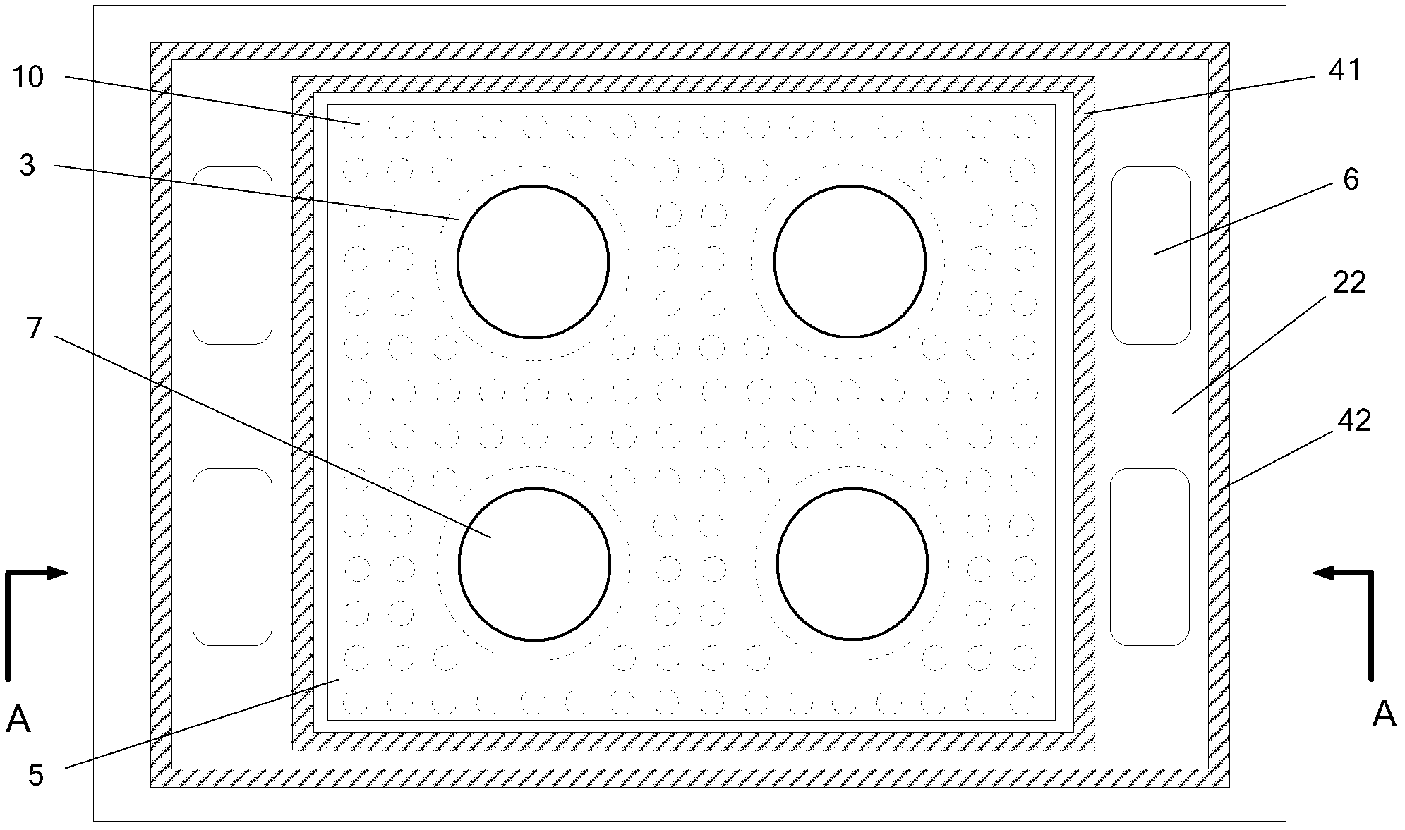
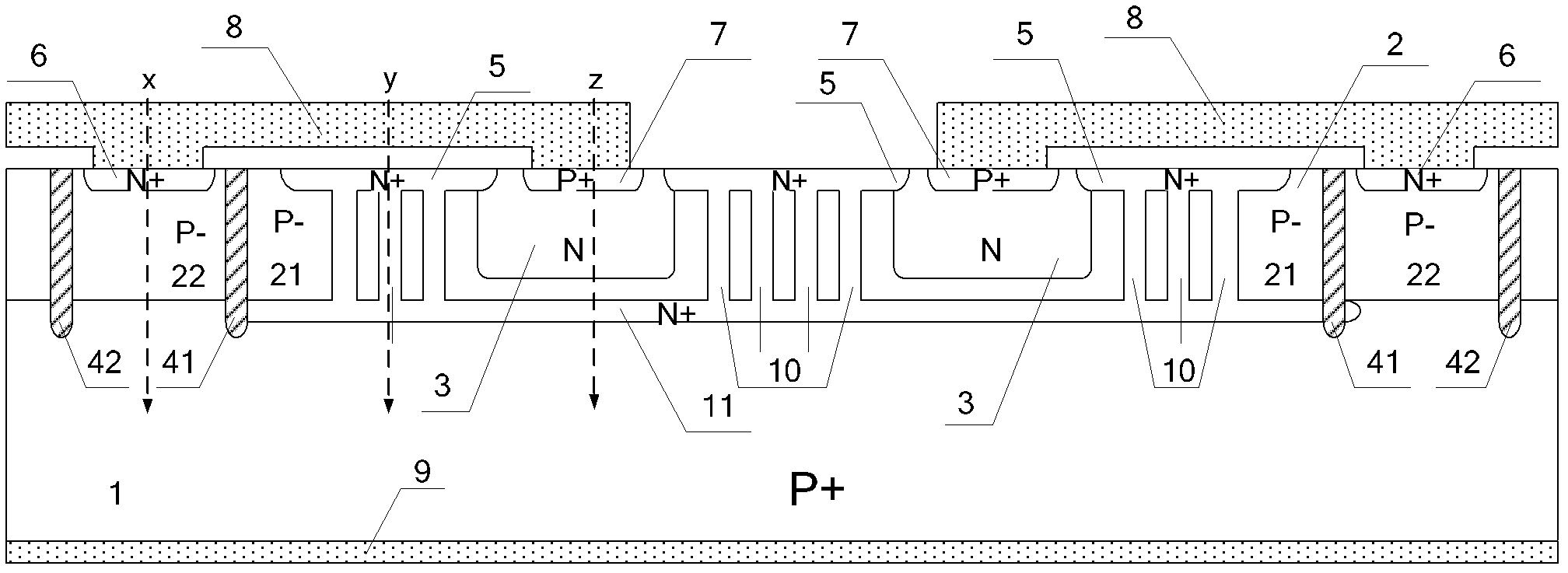
[0036] Such as figure 2 and image 3 As shown, a transient voltage suppressor based on multichannel current sharing includes a P+ substrate layer 1; a P- epitaxial layer 2 is arranged on the P+ substrate layer 1, and a ground electrode 9 is arranged at the bottom of the P+ substrate layer 1; Layer 2 is divided into two regions by the outer isolation ring 42 and the inner isolation ring 41: the first epitaxial region 21 located in the inner isolation ring 41 and the second epitaxial region 22 located between the outer isolation ring 42 and the inner isolation ring 41 ; An N+ buried layer 11 is provided between the first epitaxial region 21 and the P+ substrate layer 1, and four N+ active injection regions 6 are provided on the seco...


PUM


Abstract

The invention discloses a multi-porous channel current equalizing-based transient voltage suppressor, which comprises a P+ substrate layer and a P- epitaxial layer. An N+ buried layer is arranged between first epitaxial regions and the P+ substrate layer; second epitaxial regions are respectively provided with N+ active injection regions; N wells are respectively embedded on the first epitaxial regions; each N well is provided with a P+ active injection region; the P+ active injection regions are connected with the N+ active injection regions through metal electrodes; the N wells are connected with the N+ active injection regions respectively paved on the first epitaxial regions; and the N+ active injection regions are connected with the N+ buried layer through a plurality of porous channels in which N-type materials are respectively filled. According to the multi-porous channel current equalizing-based transient voltage suppressor disclosed by the invention, electronic static discharge (ESD) current is evenly lead to Zener junctionby adopting the multi-porous channel current equalizing technology, so that the current collected by the Zener nodes is basically the same in density, and thereby, the phenomenon that the partial failure the Zener nodes is caused because of different current densities is avoided, the area utilization ratio of the node is effectively increased, meanwhile, the on resistance is lowered, the clamping feature is improved, and the ESD resistance of devices is enhanced.

Description

technical field [0001] The invention belongs to the technical field of electrostatic protection for integrated circuits, and in particular relates to a transient voltage suppressor based on multi-channel current sharing. Background technique [0002] With the rapid development of electronic information technology, the current semiconductor devices tend to be miniaturized, high-density and multi-functional, especially for applications such as fashion consumer electronics and portable products that have strict requirements on the motherboard area, they are vulnerable to electrostatic discharge (ESD) )Impact. Static electricity exists all the time and everywhere. In the 1960s, with the emergence of MOS devices that are very sensitive to static electricity, the problem of static electricity also appeared. In the 1970s, the problem of static electricity became more and more serious. The density of the circuit is getting bigger and bigger. On the one hand, the thickness of the si...

Claims


Application Information

Patent Timeline
Patent Type & Authority Applications(China)
IPC IPC(8): H01L29/06H01L27/02
Inventor 董树荣吴健韩成功黄丽苗萌曾杰马飞郑剑锋
Owner ZHEJIANG UNIV
Why Eureka
Try Eureka