SiC-bipolar junction transistor (SiC-BJT) device for power integrated circuit and manufacturing method of SiC-BJT device

A technology of an integrated circuit and a manufacturing method, applied in the field of microelectronics, can solve the problems of large size and volume of the power module circuit, and achieve the effects of reducing the area size, reducing the interface electric field density, and improving the breakdown voltage

Inactive Publication Date: 2012-07-25
XIDIAN UNIV
View PDF5 Cites 20 Cited by
  • Summary
  • Abstract
  • Description
  • Claims
  • Application Information

AI Technical Summary

Problems solved by technology

Discrete devices cannot be integrated into the chip in integrated circuit design because the electrode positions are not on the same side, resulting in a large size and volume of the power module circuit

Method used


Image

  • SiC-bipolar junction transistor (SiC-BJT) device for power integrated circuit and manufacturing method of SiC-BJT device
  • SiC-bipolar junction transistor (SiC-BJT) device for power integrated circuit and manufacturing method of SiC-BJT device
  • SiC-bipolar junction transistor (SiC-BJT) device for power integrated circuit and manufacturing method of SiC-BJT device

Examples


Embodiment 1

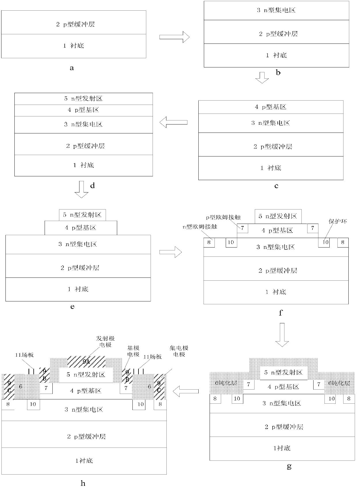
[0031] Step 1: Select a p-type SiC substrate, after cleaning, epitaxially grow a p-type buffer layer with a thickness of 2um on the p-type substrate, in which the aluminum doping concentration is 7×10 18 cm -3 ,Such as image 3 a.

[0032] Step 2: Epitaxially grow an n-type collector region with a thickness of 5um on the p-type buffer layer, in which the nitrogen doping concentration is 5×10 16 cm -3 ,Such as image 3 b.

[0033] Step 3: Epitaxially grow a p-type base region with a thickness of 1um on the n-type collector region, in which the aluminum doping concentration is 3×10 17 cm -3 ,Such as image 3 c.

[0034] Step 4: Epitaxially grow an n-type emitter region with a thickness of 1.2um on the p-type base region, where the nitrogen doping concentration is 2×10 19 cm -3 ,Such as image 3 d.

[0035] Step 5: Etch the mesa of the 1um emitter region from the uppermost n-type emitter region, and etch the mesa of the 0.8um base region from the p-type base region, s...

Embodiment 2

[0045] Step 1: Select an n-type SiC substrate, after cleaning, epitaxially grow a p-type buffer layer with a thickness of 5um on the n-type substrate, in which the aluminum doping concentration is 5×10 18 cm -3 ,Such as image 3 a.

[0046] Step 2: Epitaxially grow an n-type collector region with a thickness of 15um on the p-type buffer layer, wherein the nitrogen doping concentration is 5×10 15 cm -3 ,Such as image 3 b.

[0047] Step 3: Epitaxially grow a p-type base region with a thickness of 0.4um on the n-type collector region, in which the aluminum doping concentration is 8×10 17 cm -3 ,Such as image 3 c.

[0048] Step 4: Epitaxially grow an n-type emitter region with a thickness of 0.5um on the p-type base region, where the nitrogen doping concentration is 6×10 19 cm -3 ,Such as image 3 d.

[0049] Step 5: Etch the mesa of the 0.5um emitter region from the uppermost n-type emitter region, and etch the mesa of the 0.2um base region from the p-type base regi...

Embodiment 3

[0059] Step A: Select a p-type SiC substrate, after cleaning, epitaxially grow a p-type SiC buffer layer with a thickness of 4um and doped with aluminum ions on the p-type substrate, and its doping concentration is 3×10 18 cm -3 ,Such as image 3 a.

[0060] Step B: Epitaxially grow an n-type collector region with a thickness of 12um on the p-type buffer layer, wherein the nitrogen doping concentration is 2×10 16 cm -3 ,Such as image 3 b.

[0061] Step C: epitaxially grow a p-type base region with a thickness of 0.7um on the n-type collector region, wherein the aluminum doping concentration is 5×10 17 cm -3 ,Such as image 3 c.

[0062] Step D: Epitaxially grow an n-type emitter region with a thickness of 0.8um on the p-type base region, wherein the nitrogen doping concentration is 4×10 19 cm -3 ,Such as image 3 d.

[0063] Step E: Etch the mesa of the 0.8um emitter region from the uppermost n-type emitter region, and etch the mesa of the 0.6um base region from t...


PUM


Abstract

The invention discloses a SiC-bipolar junction transistor (SiC-BJT) device for a power integrated circuit and a manufacturing method of the SiC-BJT device and mainly aims to solve the problem that a traditional SiC-BJT cannot be used for the power integrated circuit. The SiC-BJT disclosed by the invention comprises an SiC substrate (1), a p-type buffer layer (2), an n-type collector region (3), a p-type base region (4), an n-type emitter region (5) and a passivation layer (6) which are arranged from bottom to top. P-type ohmic contacts (7) are respectively located at both sides of the p-type base region (4); n-type ohmic contacts (8) are respectively located at both sides of the n-type emitter region (5); an emitting electrode (9A) is located on the n-type emitter region (5); base electrodes (9B) are respectively located on the p-type ohmic contacts (7); collector electrodes (9C) are respectively located on the n-type ohmic contacts (8); protection rings (10) which are 0.2-0.6mum long are arranged at the position of the interface of the n-type collector region (3) and the p-type base region (4); and field plates (11) which are 0.5-1mum long are arranged on the base electrodes (9B). The SiC-BJT device for the power integrated circuit has the advantages of small size, easiness in integration and high breakdown voltage and can be used for preparing the power integrated circuit.

Description

technical field [0001] The invention belongs to the field of microelectronics, and in particular relates to a silicon carbide power device and a related manufacturing method thereof, which can be used for power integrated circuits. technical background [0002] With the establishment and promotion of the concept of green environmental protection in the world, facing the increasing energy pressure, research on energy-saving and efficient electronic devices has become an urgent concern for the semiconductor industry. 70% of the world's power consumption comes from power semiconductor devices. In many application fields, power semiconductor devices work for a long time, and some may even work twenty-four hours a day, three hundred and sixty-five days a year. Therefore, how to improve the power semiconductor Device efficiency plays a crucial role in the efficient use of electrical energy. [0003] Silicon carbide is a wide bandgap semiconductor, and the intrinsic carrier can st...

Claims


Application Information

Patent Timeline
Patent Type & Authority Applications(China)
IPC IPC(8): H01L29/73H01L29/06H01L21/04
Inventor 吕红亮宁旭斌张玉明张晓朋
Owner XIDIAN UNIV
Why Eureka
Try Eureka