Film packaging method of organic light-emitting device

An organic light-emitting device and thin-film packaging technology, which is applied in the manufacture of electric solid-state devices, semiconductor devices, and semiconductor/solid-state devices, etc., can solve the problems of unsatisfactory sealing effect, etc. Effect

Inactive Publication Date: 2012-07-25
IRICO DISPLAY DEVICES
View PDF6 Cites 20 Cited by
  • Summary
  • Abstract
  • Description
  • Claims
  • Application Information

AI Technical Summary

Problems solved by technology

Such a layer structure is for example proposed in CN 101106178A, although good results are obtained thereby, the final sealing effect is still not satisfactory

Method used


Image

  • Film packaging method of organic light-emitting device
  • Film packaging method of organic light-emitting device
  • Film packaging method of organic light-emitting device

Examples


Embodiment 1

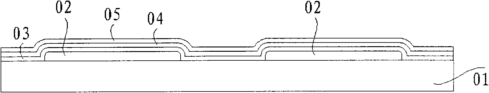
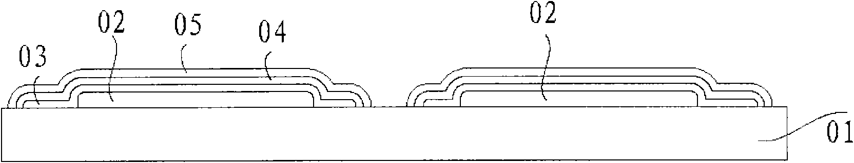
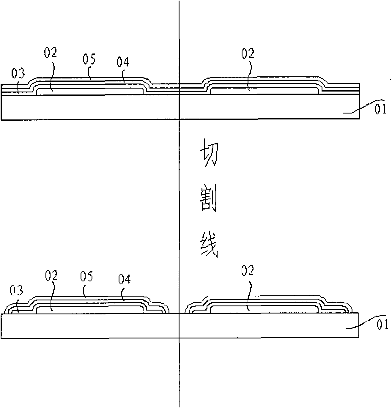
[0021] The present invention utilizes mask plate technology in the process of depositing thin film, makes deposited thin film produce such as figure 2 The sealing effect shown is that the upper sealing layer completely wraps the edge of the lower sealing layer to form individual sealing units. The mask plate is made of nickel steel, the pattern of the mask plate is consistent with the pattern of a single organic light-emitting device, and the size of the mask plate used for the thin film sealing layer 03 / 04 / 05 is increased by 50 microns sequentially.

[0022] The first step: Deposit the inorganic thin film sealing layer 03, this layer is deposited by ion beam sputtering, and the sealing material is Al 2 o 3 , the deposition chamber is 10 -6 The vacuum degree is Pa, the deposition time is 3min, and the deposition thickness is 15nm.

[0023] Put the substrate 01 into the deposition chamber, place the first mask on the corresponding position of the substrate 01, adjust the vac...

Embodiment 2

[0036] The first step: deposit the inorganic thin film sealing layer 03, this layer is deposited by magnetron sputtering, and the sealing material is Al 2 o 3 , the deposition chamber is 10 -6 The vacuum degree is Pa, the deposition time is 5min, and the deposition thickness is 50nm.

[0037] Put the substrate 01 into the deposition chamber, place the first layer of mask on the corresponding position of the substrate 01, adjust the vacuum degree in the deposition chamber and set the deposition time, complete the deposition after 5 minutes, and take out the first layer of mask Plate, replace the second mask plate.

[0038] This step completes the preparation of the inorganic thin film sealing layer 03 on the substrate 01 .

[0039] The second step: deposit organic thin film sealing layer 04, this layer adopts chemical vapor deposition (CVD), the sealing material adopts polyurea, and the deposition chamber is 10 -6 The vacuum degree is Pa, the deposition time is 10min, and t...

Embodiment 3

[0048] The first step: Deposit inorganic sealing layer 03, this layer is deposited by magnetron sputtering, the sealing material is SiN, and the vacuum degree in the deposition chamber is 10 -5 Pa, the deposition time is 3min, and the deposition thickness is 30nm.

[0049] Put the substrate 01 into the deposition chamber, place the first mask plate (10) on the corresponding position of the substrate 01, adjust the vacuum degree in the deposition chamber and set the deposition time, after 3 minutes to complete the deposition, take out the first Layer mask, replace with the second layer mask.

[0050] This step completes the preparation of the inorganic sealing layer 03 on the substrate 01 using SiN material.

[0051] The second step: deposit organic thin film sealing layer 04, this layer adopts chemical vapor deposition (CVD), the sealing material adopts C-type polychlorinated p-xylene, and the vacuum degree in the deposition chamber is 10 -5 Pa, the deposition time is 20min,...


PUM

PropertyMeasurementUnit
thicknessaaaaaaaaaa
thicknessaaaaaaaaaa
thicknessaaaaaaaaaa

Abstract

The invention provides a film packaging method of an organic light-emitting device, at least three film sealing layers are deposited on a baseboard from bottom to top, wherein inorganic material and organic material are alternatively deposited on each film sealing layer; a chemical vapor deposition method is preferentially carried out on the organic film sealing layer, and an iron beam sputtering method or an atomic layer deposition method or an magnetron sputtering deposition can be carried out on the inorganic film sealing layer; the early deposited film sealing layer is thinner than the film sealing layer deposited latter; different mask plates are adopted to deposit each film sealing layer, the geometry sizes of the patterns of the mask plates of the first layer, the second layer and the third layer increase sequentially. According to the film packaging method of the organic light-emitting device, the crack caused by plate breaking can be effectively reduced, the space between the sealing layer and the baseboard can be prevented from tilting resulting in air leakage during cutting, and the service life of the device can be effectively prolonged.

Description

technical field [0001] The invention relates to a preparation process of an organic light emitting diode display device (OLED), in particular to a film packaging method of an organic light emitting device. Background technique [0002] In recent years, organic light-emitting diodes (OLEDs), which are self-luminous devices, have attracted widespread attention as flat panel display devices. The lifetime of an OLED device depends on the selected organic material on the one hand, and on the packaging method of the device on the other hand. For organic electronic devices, especially OLEDs, it is necessary to strictly prevent oxygen and moisture from the surrounding environment from entering the device and contacting sensitive organic substances and electrodes. Because inside the OLED device, the existence of moisture or oxygen can easily cause the degradation or failure of its characteristics, and even a small amount of moisture will peel off the organic compound layer and the e...

Claims


Application Information

Patent Timeline
Patent Type & Authority Applications(China)
IPC IPC(8): H01L51/56H01L51/52
Inventor 张斌
Owner IRICO DISPLAY DEVICES
Why Eureka
Try Eureka