
Thin-film solar cell and manufacturing method therefor

A technology of solar cells and thin films, applied in circuits, photovoltaic power generation, electrical components, etc., can solve the problems of increased Joule loss, longer current path, and too large bending of the scribing line, so as to reduce the electric field intensity. Effects of suppressing Joule loss and improving power generation efficiency

Inactive Publication Date: 2015-04-15
MITSUBISHI ELECTRIC CORP
View PDF4 Cites 0 Cited by
  • Summary
  • Abstract
  • Description
  • Claims
  • Application Information

AI Technical Summary

Problems solved by technology

[0007] In addition, even if the width of the unit cell is enlarged and reduced and most of the current flows through the short current path in the transparent electrode to reduce the overall resistance loss as in Patent Document 1, there are disadvantages such as the following: Compared with the case where the scribed track forms a unit cell, the current path in the transparent electrode sometimes becomes longer in the portion where the width of the unit cell is enlarged; part, the electric field strength becomes higher, so the Joule loss becomes larger; in the case of making the width of the unit cell expand and shrink as in Patent Document 1, it is necessary to set the minimum width of the unit cell to a positive value, so the same as Compared with the case of forming a unit cell with scribed lanes parallel to each other, the curvature of the scribed lanes cannot be made too large

Method used


Image

  • Thin-film solar cell and manufacturing method therefor
  • Thin-film solar cell and manufacturing method therefor
  • Thin-film solar cell and manufacturing method therefor

Examples


Embodiment approach 1

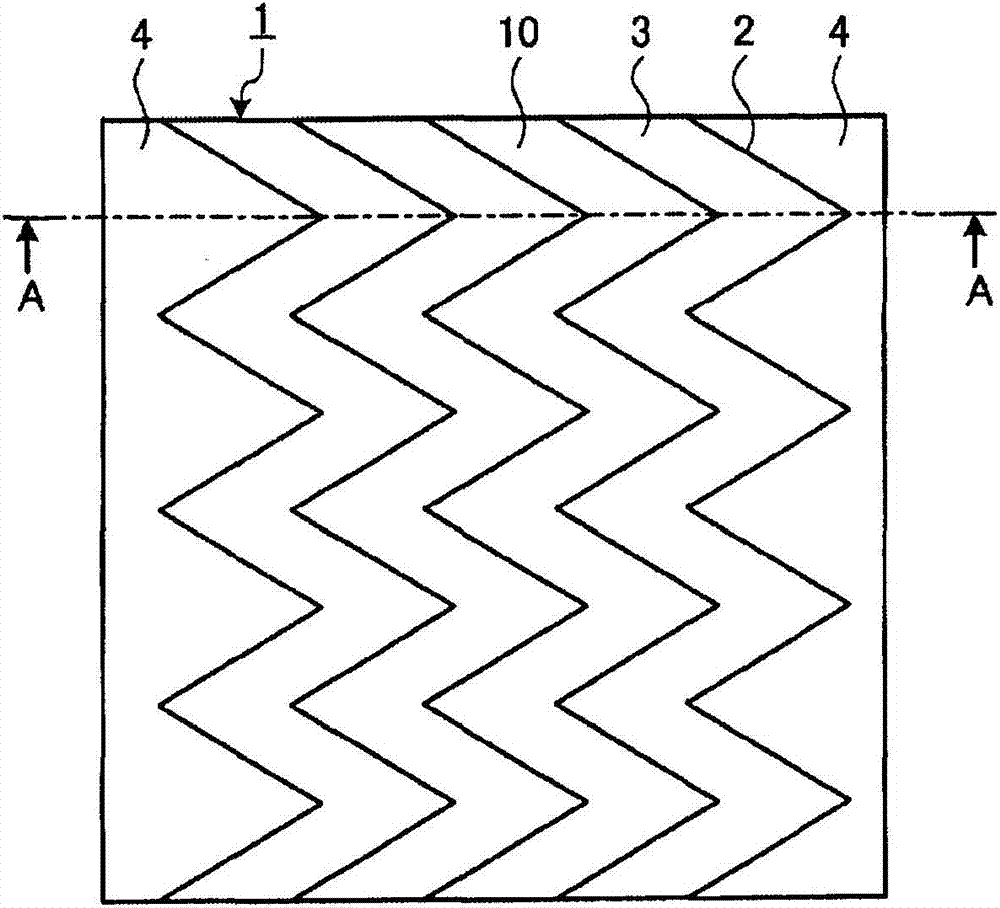
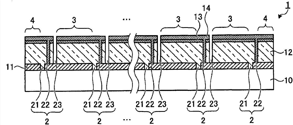
[0041] figure 1It is a plan view showing an example of the thin-film solar cell according to Embodiment 1 of the present invention. The thin-film solar cell 1 according to Embodiment 1 is integrated by connecting a plurality of unit solar cells 3 in series on a rectangular insulating and translucent substrate 10 , thereby functioning as a thin-film solar cell module as a whole. Furthermore, the current led to the current extraction parts 4 at both ends is extracted to the outside. Here, between the unit solar cells 3 and between the unit solar cells 3 and the current extraction part 4, they are separated by the scribe line 2 as a separation groove. Combinations of line segments whose end faces of the optical substrate 10 are inclined are periodically repeated in a curved shape, and adjacent scribe lanes 2 are arranged substantially parallel to each other. In addition, the unit solar cell 3 has a shape in which the direction along the scribed lane 2 becomes the lengthwise dir...

Embodiment approach 2

[0127] Figure 16It is a plan view showing an example of the thin-film solar cell according to Embodiment 2 of the present invention. Thin-film solar cell 1 according to Embodiment 2 has a structure in which scribe lanes 2 are arranged with a degree of curvature decreasing from the center of insulating translucent substrate 10 toward the edge (end) of the width direction of scribe lane 2 . In this example, the shape of the scribe line 2 separating the unit solar cell 3 and the current extraction part 4 at both ends in the width direction is substantially parallel to the end surface of the insulating translucent substrate 10 . In addition, since the degree of curvature of adjacent scribe lanes 2 at the edge varies, they are not substantially parallel, but the positions and periods of the peaks and valleys constituting the curved portion are consistent. Accordingly, it is possible to suppress occurrence of a site where the amount of change in the width of the unit solar battery...

Embodiment approach 3

[0132] Figure 17 It is a plan view showing an example of the thin-film solar cell according to Embodiment 3 of the present invention. In the thin-film solar cell 1 according to Embodiment 3, the degree of curvature of the scribe lane 2 does not change even at the edge (end) of the scribe lane 2 in the width direction. When the scribed lane 2 at the end is intended to be substantially parallel to the adjacent scribed lane 2 , it will protrude from the insulating translucent substrate 10 . Therefore, the curved portion of the endmost scribe line 2 protruding from the insulating and translucent substrate 10 is parallel to the end surface of the insulating and translucent substrate 10 so as to converge in the insulating and translucent substrate 10 . In addition, the shape of the scribed lane 2 is changed so that the unit solar cells 3 arranged at both ends in the left-right direction of the drawing (the width direction of the scribed lane 2 ) have approximately the same area as...


PUM


Abstract

A thin film solar cell includes, on a substrate, a first electrode layer formed of a transparent conductive material, a photoelectric conversion layer, and a second electrode layer including a conductive material that reflects light. The thin film solar cell includes a plurality of unit solar battery cells divided by scribe lines. The second electrode layer and the first electrode layer of the unit solar battery cell adjacent to the second electrode layer are connected in the scribe line formed in the photoelectric conversion layer. The unit solar battery cells are electrically connected in series. The scribe lines on both sides of at least one of the unit solar battery cells are formed such that the unit solar battery cell held between the scribe lines meanders while having fixed width in a predetermined direction and have same shapes that overlap when the scribe lines translate in the predetermined direction.

Description

technical field [0001] The invention relates to a thin-film solar cell and a manufacturing method thereof. Background technique [0002] Solar power generation system as protection of the global environment in the 21st century from CO caused by burning fossil energy 2 The clean energy of the influence of the increase of the gas is expected, and the production amount thereof is explosively increased in the world. Therefore, a shortage of silicon wafers occurs in the world. Therefore, in recent years, the production volume of thin-film solar cells in which the photoelectric conversion layer (semiconductor layer) is formed of a thin film has rapidly increased without being restricted by the supply amount of silicon wafers. [0003] In thin-film solar cells, transparent electrodes and photoelectric conversion layers of thin films are directly formed on a substrate with a large area of ​​about one meter square by sputtering, evaporation, and CVD (Chemical Vapor Deposition: Chem...

Claims


Application Information

Patent Timeline
Patent Type & Authority Patents(China)
IPC IPC(8): H01L31/0352H01L31/18
CPCH01L31/035272H01L31/0463Y02E10/50
Inventor 仲村惠右时冈秀忠古畑武夫
Owner MITSUBISHI ELECTRIC CORP
Learn More