Method for increasing bonding force between conductive body and non-conductive macromolecule dielectric layer in printed circuit board substrate

A printed circuit and conductor technology, which is applied in the secondary treatment of printed circuits, improvement of metal adhesion of insulating substrates, coatings, etc.

Inactive Publication Date: 2012-08-01
DONGGUAN RENJI ELECTRONICS MATERIAL +1
View PDF3 Cites 6 Cited by
  • Summary
  • Abstract
  • Description
  • Claims
  • Application Information

AI Technical Summary

Problems solved by technology

[0008] Cu 2 0 It is easy to form long needle-like or feather-like crystals, which are easy to break at high temperatures and greatly affect the adhesion between copper and resin, and cause black spots to disperse in the wrench with glue flow to form electrical problems, and are also prone to moisture And after the formation of high heat, local delamination explosion

Method used


Image

  • Method for increasing bonding force between conductive body and non-conductive macromolecule dielectric layer in printed circuit board substrate
  • Method for increasing bonding force between conductive body and non-conductive macromolecule dielectric layer in printed circuit board substrate
  • Method for increasing bonding force between conductive body and non-conductive macromolecule dielectric layer in printed circuit board substrate

Examples


Embodiment Construction

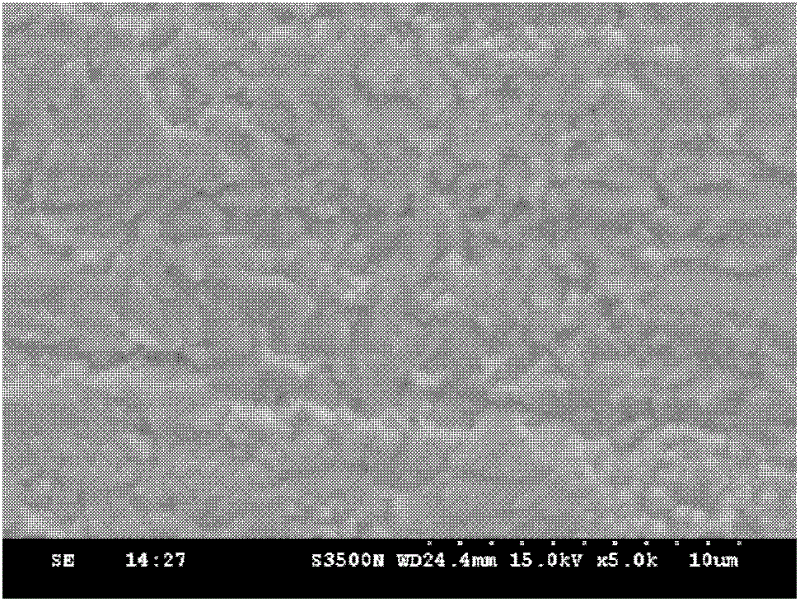
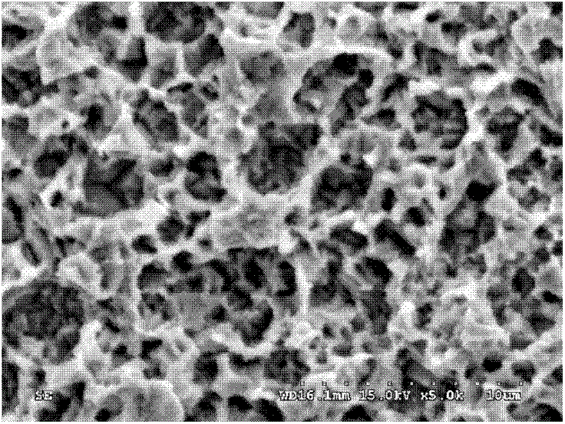
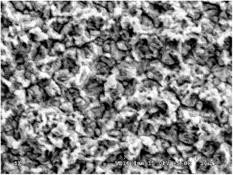
[0067] With the development of electronic products in the direction of thinner and lighter, coupled with dense electronic circuits, the roughness of the inner metal plate, that is, the conductor, is reduced, which in turn leads to the reliability of the bonding force. On the other hand, halogen-free flame retardants gradually replace halogen flame retardants and become the main substrate of printed circuits. At present, non-conductive polymer dielectric layer materials commonly used in the electronics industry have FR-4, insulation, halogen-free, High Tg Features, mainly made of glass fiber and epoxy resin or phenol resin, such as polytetrafluoroethylene (PTFE), epoxy resin (EPOXY RESIN), polyimide (POLYIMIDE), Polycyanate resin (POLYCYANATE ESTER), butylene terephthalate resin (BUTADIENE TEREPHTHALATE RESIN) or a mixture of the above materials, etc. In order to improve the metal plate, that is, the conductor, the surface roughness and the bonding force, the present invention ...


PUM


Abstract

The invention provides a method for increasing bonding force between a conductive body and a non-conductive macromolecule dielectric layer in a printed circuit board substrate. The method comprises the steps of performing rough treatment to the surface of the conductive body, soaking the conductive body in a silane solution with 0.01%-100% of volume concentration for seconds or minutes after the rough treatment or directly spraying the silane solution with 0.01%-100% of volume concentration onto the surface of the conductive body, and accordingly adding a silane layer on the surface. On the basis of existing methods, the method increases a process for forming the silane layer in one step, thereby increasing the bonding force between the conductive body and the non-conductive macromolecule dielectric layer and solving the board exploding problem caused by insufficient bonding force between the conductive body and the non-conductive macromolecule dielectric layer.

Description

technical field [0001] The invention relates to a printed circuit board substrate, in particular to a method for increasing the binding force between a conductor and a non-conductive polymer dielectric layer in the printed circuit board substrate. Background technique [0002] As the carrier of various components and the hub of circuit signal transmission, printed circuit board (PCB) has become the most important part of electronic information products. With the miniaturization of electronic information products and the environmental protection requirements of lead-free and halogen-free, PCB is also developing in the direction of high density, high glass transition point (Tg) and environmental protection. Especially in recent years, with the enhancement of people's awareness of environmental protection, halogen flame retardants are used as the main substrate of printed circuit boards, and the combustion products of their waste release dioxins (Dioxin), dibenzofuran (Dibenxof...

Claims


Application Information

Patent Timeline
Patent Type & Authority Applications(China)
IPC IPC(8): C09D183/04C09D183/08H05K3/38
Inventor 王维仁
Owner DONGGUAN RENJI ELECTRONICS MATERIAL
Why Eureka
Try Eureka