
Post chemical-mechanical polishing (CMP) cleaning method and CMP method

A chemical mechanical and post-cleaning technology, which is applied in the field of chemical mechanical grinding and cleaning, can solve the problems of easy sticking to the clean polysilicon surface, re-contamination, etc., achieve good cleaning effect and improve etching efficiency.

Inactive Publication Date: 2012-08-01
SHANGHAI HUAHONG GRACE SEMICON MFG CORP
View PDF4 Cites 6 Cited by
  • Summary
  • Abstract
  • Description
  • Claims
  • Application Information

AI Technical Summary

Problems solved by technology

[0008] However, for cleaning after CMP of source polysilicon, NH 4 Wafers with OH or standard SCl will maintain a clean polysilicon surface, or only form a less oxide layer on the polysilicon surface, so that, in the subsequent PVA brush cleaning step, the organic contamination particles on the PVA brush can easily stick to the surface of the polysilicon. clean polysilicon surface, so it will cause recontamination

Method used


Image

  • Post chemical-mechanical polishing (CMP) cleaning method and CMP method
  • Post chemical-mechanical polishing (CMP) cleaning method and CMP method
  • Post chemical-mechanical polishing (CMP) cleaning method and CMP method

Examples


Embodiment Construction

[0020] In order to make the content of the present invention clearer and easier to understand, the content of the present invention will be described in detail below in conjunction with specific embodiments and accompanying drawings.

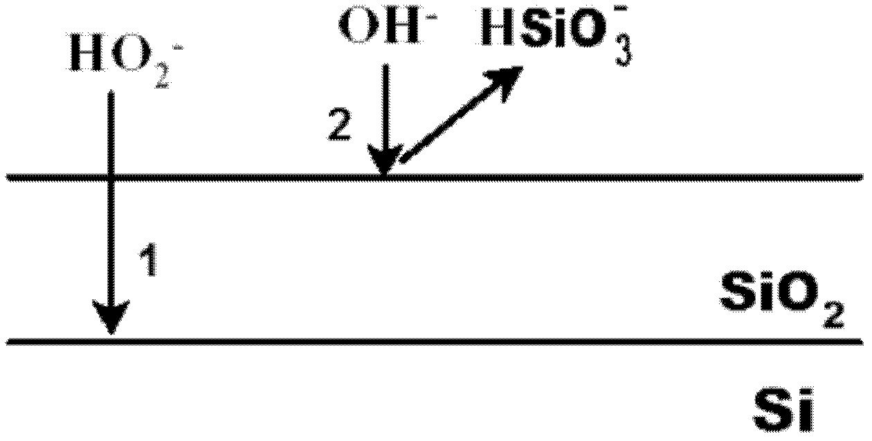
[0021] In prior art, NH in SCl solution 4 The mass percentage of OH is generally 2.0%+ / -0.2%, H 2 o 2 The mass percentage is generally 2.0%+ / -0.2%. Among them, the etchant in the SCl solution is NH 4 Oh.

[0022] Different from the above concentration of the prior art, the NH in the SCl solution 4 The mass percentage of OH is changed to 2.8+ / -0.2%; H 2 o 2 The mass percent was changed to 3.0+ / -0.2%.

[0023] That is, in the cleaning method after chemical mechanical polishing according to an embodiment of the present invention, first, in the megasonic cleaning step, using NH 4 The mass percentage of OH is 2.8+ / -0.2%, H 2 o 2 The SCl solution with a mass percentage of 3.0+ / -0.2% is used for megasonic cleaning; thereafter, in the PVA scru...


PUM


Abstract

The invention provides a post chemical-mechanical polishing (CMP) cleaning method for polysilicon and a CMP method. The post CMP cleaning method provided by the invention comprises the steps that firstly, in a megasonic cleaning step, an H2O2-rich SC1 solution in which the mass percentage of NH4OH is 2.8 plus / minus 0.2 percent and the mass percentage of H2O2 is 3.0 plus / minus 0.2 percent is utilized to conduct megasonic cleaning; and afterwards, in a subsequent polyvinyl alcohol (PVA) brush cleaning step, NH4OH (ammonia water) and deionized water (DIW) are utilized to clean a wafer and brush the surface of the wafer. According to the post CMP cleaning method, the high concentration SC1 solution (in which the NH4OH serves as an etching agent) is utilized to improve the etching efficiency of a natural oxide layer, so that a better cleaning effect can be achieved; meanwhile, the H2O2 with higher concentration in the SC1 solution is utilized to oxidize the polysilicon to form the oxide layer, so that the natural oxide layer of a certain thickness can be generated on the surface of the polysilicon while the better effect is achieved, an organic pollutant layer cannot be formed on the polysilicon in the subsequent brush cleaning process, and the growth of the natural oxide layer of the polysilicon in the air cannot be influenced by pollutants on the polysilicon.

Description

technical field [0001] The present invention relates to a semiconductor manufacturing method, more specifically, the present invention relates to a cleaning method after chemical mechanical polishing and a chemical mechanical polishing method using the cleaning method after chemical mechanical polishing. Background technique [0002] For flash memory products, the source polysilicon will form a native oxide layer after chemical mechanical polishing. An etch-back of the source polysilicon can then be performed with a high selectivity to polysilicon and oxide, specifically about 30:1. Even a small change in the native oxide layer can greatly affect the amount of polysilicon etch back, resulting in critical dimension deviation. [0003] Generally, in the air at room temperature, the natural oxide layer on the polysilicon surface of the flash memory grows very rapidly, is easy to reach saturation, and is very uniform. However, when the polysilicon surface of the flash memory i...

Claims


Application Information

Patent Timeline
IPC IPC(8): H01L21/02B08B3/04
Inventor 李儒兴秦海燕李志国龚大伟王雷
Owner SHANGHAI HUAHONG GRACE SEMICON MFG CORP
Learn More