Micro-ring assistant ring mirror structure

A micro-ring and ring-mirror technology, applied in the directions of light guides, optics, instruments, etc., can solve the problems of unachievable, unapplied wavelength selection, complicated fabrication, etc., achieve good process compatibility, increase wavelength (or frequency) tunable Function, effect of large wavelength tunable range

Inactive Publication Date: 2014-11-12
ZHEJIANG UNIV
View PDF10 Cites 0 Cited by
  • Summary
  • Abstract
  • Description
  • Claims
  • Application Information

AI Technical Summary

Problems solved by technology

In integrated optics technology, high-efficiency optical path reflection is achieved. Simple end-face reflection requires the production of high-reflection film, which is complex and often impossible to achieve. Bragg gratings are the most commonly used reflection structures. The problem is that the production of gratings has special requirements. The frequency selection of the grating is not adjustable; the ring mirror is also a common structure. The advantage is that the production is the same process as the general waveguide structure, and there is no special requirement. However, in certain applications, it cannot be used for wavelength selection.

Method used


Image

  • Micro-ring assistant ring mirror structure
  • Micro-ring assistant ring mirror structure
  • Micro-ring assistant ring mirror structure

Examples


Embodiment 1

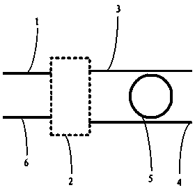
[0035] like figure 2 As shown, the device adopts a symmetrical Y branch structure 12 as a beam splitting coupling structure. The device is made of silicon-on-insulator (SOI) material, the thickness of the top silicon layer is 220 nm, and the thickness of the silicon dioxide buried layer is 1 μm. Using CMOS technology, through deep ultraviolet lithography and silicon dry etching, a ridge-shaped optical waveguide with a width of 400nm and a depth of 180nm is fabricated to form a figure 2 The device structure shown. The optical microring in the device is an optical waveguide ring with a radius of 5 μm. The gap between the microring and the two parallel waveguides is 180 nm. The Y branch structure is composed of S-shaped bends with a length of 25 μm.

[0036] After silicon dry etching is completed, a 1 μm silicon dioxide layer is covered by chemical vapor deposition. By sputtering, photolithography, and etching, the heating electrodes corresponding to the microrings are fab...

Embodiment 2

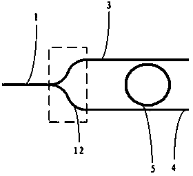
[0039] like Figure 4 As shown, the device uses a symmetrical X-cross junction structure 22 as the beam splitting coupling structure. The device is made of glass. Using buried ion exchange technology, a buried optical waveguide with a width of 10 μm and a depth of 18 μm is produced, forming Figure 4 The device structure shown. The optical microring in the device is a racetrack-shaped optical waveguide closed loop with a radius of 5 mm. The gap between the microring and the two parallel waveguides is 3 μm. The widths of the asymmetric side waveguides of the X-cross junction structure are 8 μm and 12 μm, respectively, and the branch angle is 0.1 degree. The width of the symmetrical side waveguide is 10 μm, and the branch angle is 1 degree.

[0040] Thus, the auxiliary ring mirror with micro ring is completed. The ring mirror does not need to use the fine process required for Bragg grating production, has a reflectivity of 98%, and the Q value of the filter spectrum is grea...

Embodiment 3

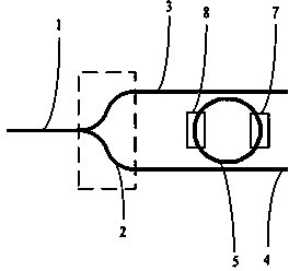
[0042] like Figure 5 As shown, the device uses a directional coupler structure 32 as a beam splitting coupling structure. The device is made of lithium niobate. Using titanium diffusion technology, a diffused optical waveguide with a width of 6 μm is produced to form a Figure 5 The device structure shown. The optical microring in the device is an optical waveguide ring with a radius of 500 μm. The gap between the microring and the two parallel waveguides is 2 μm. The waveguide gap of the directional coupler structure is 3 μm, and the length is 500 μm.

[0043] Thus, the auxiliary ring mirror with micro ring is completed. The ring mirror does not need to use the fine process required for Bragg grating production, has a reflectivity of 98%, and the Q value of the filter spectrum is greater than 1500.


PUM


Abstract

The invention discloses a micro-ring assistant ring mirror structure. The ring mirror structure comprises two input waveguides, a 1*2 or 2*2 beam splitting coupled structure, a closed-ring-shaped light micro ring and two parallel straight waveguides, wherein one end of the beam splitting coupled structure is connected with the two input waveguides, and the other end of the beam splitting coupled structure is connected with the two parallel straight waveguides; and the closed-ring-shaped light micro ring is placed between the two parallel straight waveguides and is coupled with the two parallel straight waveguides, and the closed-ring-shaped light micro ring and the two parallel straight waveguides are positioned on the same plane. According to the ring mirror structure, the micro ring characteristic is utilized, the reflex function is guaranteed, meanwhile the ring mirror structure has good wavelength (or frequency) selection function and combines a wavelength tunable function of a micro ring, the ring mirror structure has larger wavelength adjusting range and is used as a practical key structure to be applied on a photovoltaic integration chip; and compared with the conventional bragg grating, on one hand, the ring mirror structure has good process compatibility, on other hand, and the wavelength (or frequency) adjustable function is added for the ring mirror structure.

Description

technical field [0001] The invention relates to an integrated optical device, in particular to a ring mirror structure assisted by a micro ring. Background technique [0002] Integrated optical technology is an important direction for the development of optical device integration. In integrated optics technology, high-efficiency optical path reflection is achieved. Simple end-face reflection requires the production of high-reflection film, which is complex and often impossible to achieve. Bragg gratings are the most commonly used reflection structures. The problem is that the production of gratings has special requirements. The frequency selection of the grating is not adjustable; the ring mirror is also a common structure. The advantage is that the production is the same process as the general waveguide structure, and there is no special requirement. However, in certain applications, it cannot be used for wavelength selection. Contents of the invention [0003] Aiming at...

Claims


Application Information

Patent Timeline
Patent Type & Authority Patents(China)
IPC IPC(8): G02B6/287
Inventor 朱冰青胡挺杨龙志周强江晓清杨建义
Owner ZHEJIANG UNIV
Why Eureka
Try Eureka