Method for improving reading redundancy of static random access memory

A technology of static randomness and redundancy, applied in the field of microelectronics, can solve the problems such as the negative effect of the electron mobility of NMOS devices, and achieve the effects of improving readout redundancy, reducing potential, and increasing equivalent resistance

Active Publication Date: 2012-09-05
SHANGHAI HUALI MICROELECTRONICS CORP
View PDF4 Cites 0 Cited by
  • Summary
  • Abstract
  • Description
  • Claims
  • Application Information

AI Technical Summary

Problems solved by technology

However, since the compressive stress in the channel will have a negative effect on the electron mobility of the NMOS device, generally speaking, the embedded silicon germanium process will not embed silicon germanium to the source and drain of the NMOS device.

Method used


Image

  • Method for improving reading redundancy of static random access memory
  • Method for improving reading redundancy of static random access memory
  • Method for improving reading redundancy of static random access memory

Examples


Embodiment Construction

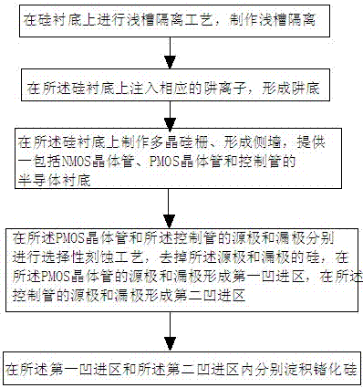
[0024] The present invention will be further described below in combination with principle diagrams and specific operation examples.

[0025] see image 3 Shown, a kind of method of improving SRAM read redundancy of the present invention, specifically comprises the following steps:

[0026] Step S1: performing shallow trench isolation (STI) on the silicon substrate to form shallow trench isolation;

[0027] Step S2: Implanting well ions on the silicon substrate to form a well bottom;

[0028] In this step, according to the different types of semiconductor devices to be formed, the formed wells are also different. For example, to manufacture a PMOS type device, it is necessary to implant boron ions into the silicon substrate to form a P well. For NMOS type devices, phosphorus ions need to be implanted into the silicon substrate to form an N well.

[0029] Step S3: performing polysilicon gate fabrication and sidewall formation on the silicon substrate respectively.

[0030] ...


PUM


Abstract

The invention discloses a method for improving the reading redundancy of a static random access memory. The method comprises the following steps of: providing a semiconductor substrate comprising an NMOS (N-channel metal oxide semiconductor) transistor, a PMOS (P-channel metal oxide semiconductor) transistor and a control tube; respectively carrying out selective etching on the source electrodes and the drain electrodes of a PMOS region and a control tube region so as to remove silicon of the source electrode and the drain electrode; forming a first sinking region on the source electrode and the drain electrode of the PMOS region, and forming a second sinking region on the source electrode and the drain electrode of the control tube; and respectively depositing silicon germanium in the first sinking region and the second sinking region. According to the invention, the carrier mobility of a control tube device is reduced while the existing process steps are not added, thereby increasing the equivalent resistance of the control tube and then reducing the potential of a node in the reading process so as to improve the reading redundancy of the random access memory.

Description

technical field [0001] The invention relates to the field of microelectronics, in particular to a method for improving the readout redundancy of a static random access memory. Background technique [0002] Static random access memory (SRAM), as an important product in semiconductor memory, has been widely used in high-speed data exchange systems such as computers, communications, and multimedia. [0003] Such as figure 1 as shown in figure 1 It is a layout structure of a common SRAM cell below 90 nanometers, including three levels of active regions, polysilicon gates, and contact holes. The area 1 marked in the figure is the control transistor (Pass Gate), which is an NMOS device, and the area 21 is marked as the pull-down transistor (Pull Down MOS), which is also an NMOS device, and the area 22 is marked The one that comes out is the pull-up tube (Pull Up MOS), and the device is a PMOS device. [0004] Readout redundancy is an important parameter to measure the readout ...

Claims


Application Information

Patent Timeline
Patent Type & Authority Applications(China)
IPC IPC(8): H01L21/8244
Inventor 俞柳江
Owner SHANGHAI HUALI MICROELECTRONICS CORP
Why Eureka
Try Eureka