SiC epitaxial wafer and method for manufacturing same
A technology of epitaxial wafers and manufacturing methods, applied in chemical instruments and methods, semiconductor/solid-state device manufacturing, crystal growth, etc., can solve problems such as heterogeneous polytype, stacking defects, dislocations, etc.
- Summary
- Abstract
- Description
- Claims
- Application Information
AI Technical Summary
Problems solved by technology
Method used
Image

Examples
Embodiment 1)
[0196] An epitaxial layer of SiC was formed on the Si face of a 4H-SiC single crystal substrate inclined at an off angle of 4°.
[0197] In this example, no convex processing was performed on the 4H-SiC single crystal substrate.
[0198] In the grinding process, the mechanical grinding before CMP uses abrasive grains with a diameter of 5 μm or less, and the processing pressure is 350 g / cm 2 conduct. In addition, CMP was carried out for 30 minutes using silica particles with an average particle diameter of 10 to 150 nm as abrasive particles, an abrasive slurry containing sulfuric acid as an inorganic acid, and having a pH of 1.9 at 20° C. Thereby, the lattice disorder layer on the surface is made to be 3 nm or less.
[0199] After the polished substrate is RCA washed, it is introduced into the growth device. Furthermore, the so-called RCA cleaning is a wet cleaning method generally used for Si wafers. It uses a solution mixed with sulfuric acid-ammonia-hydrochloric acid and ...
Embodiment 2)
[0211] A SiC epitaxial wafer was produced under the same production conditions as in Example 1 except that the growth process was performed at a growth rate of 4 μm / hour for 2.5 hours.
[0212] For the SiC epitaxial wafer produced, an optical surface inspection device (Candela CS20 manufactured by KLA-Tencor Corporation), a photoluminescence imaging device (PLI-100 manufactured by Photondezin Corporation) and a wide-range observation type AFM (manufactured by Keyence Corporation) were used. Nanoscale Hybrid Microscope VN-8000) for measurement and evaluation.
[0213] Triangular defect density is 0.4 / cm 2 , the laminated defect density is 0.1 / cm 2 .
[0214] In addition, no step bundles were observed.
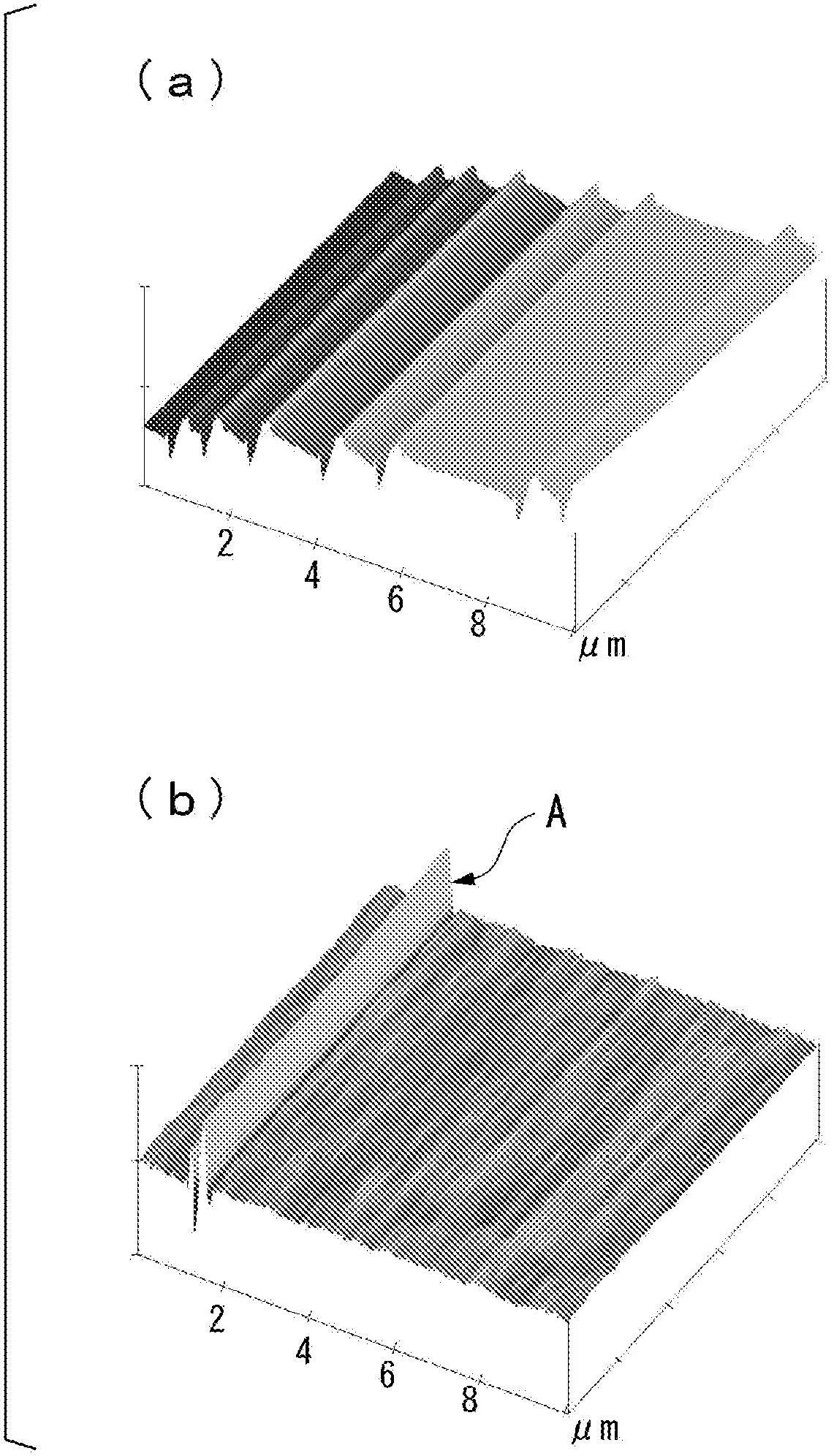
[0215] All are 1 piece / cm 2 Hereinafter, an extremely high-quality epitaxial film with a low defect density was also formed on the 4H-SiC single crystal substrate having a lower off angle of 1.2° than in Example 1.
[0216] [C-plane of 4H-SiC single crystal substrate with o...
Embodiment 3)
[0218] Using a multi-wire saw, slice the Si surface into a convex shape so that the radius of curvature of the convex part becomes 50 m, and implement the growth process for 2.5 hours at a growth rate of 4 μm / hour, under the same production conditions as in Example 1. Made SiC epitaxial wafers.
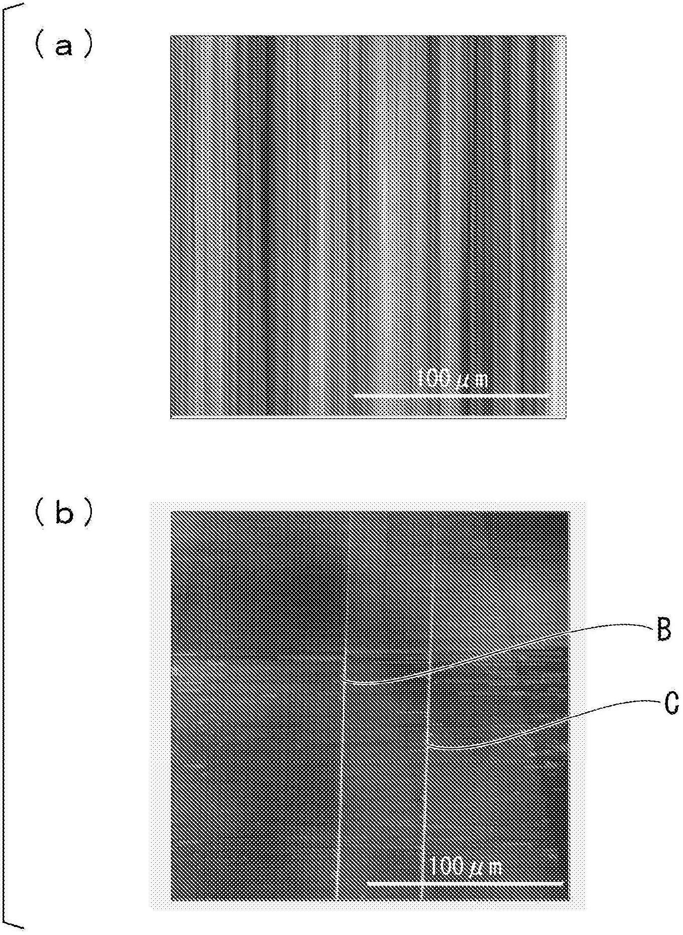
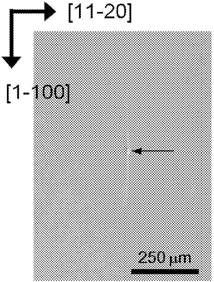
[0219] The obtained SiC epitaxial wafers were measured using an optical surface inspection device (Candela CS20 manufactured by KLA-Tencor Corporation) and a photoluminescence imaging device (PLI-100 manufactured by Photondezin Corporation), respectively. Figure 9 shown. Triangular defect density is 0.4 / cm 2 , the laminated defect density is 0.2 / cm 2 . All are 1 piece / cm 2 Next, an extremely high-quality epitaxial film with a low defect density was formed also on the Si surface of a 4H-SiC single crystal substrate with a low off-angle.
[0220] In addition, in the measurement of the optical surface inspection device (Candela CS20 manufactured by KLA-Tencor Corporation) and the w...
PUM
| Property | Measurement | Unit |
|---|---|---|
| radius | aaaaa | aaaaa |
| size | aaaaa | aaaaa |
| height | aaaaa | aaaaa |
Abstract
Description
Claims
Application Information
 - R&D
- Intellectual Property
- Life Sciences
- Materials
- Tech Scout
- Unparalleled Data Quality
- Higher Quality Content
- 60% Fewer Hallucinations
Browse by: Latest US Patents, China's latest patents, Technical Efficacy Thesaurus, Application Domain, Technology Topic, Popular Technical Reports.
© 2025 PatSnap. All rights reserved.Legal|Privacy policy|Modern Slavery Act Transparency Statement|Sitemap|About US| Contact US: help@patsnap.com