Method for preparing structured graphene based on reaction of Cl2 and Ni film annealing

A graphene and structured technology, applied in the field of microelectronics, can solve the problems of strong interaction between graphene sheets and substrates, loss of single-layer graphene properties, poor continuity of graphene, etc., and achieve low cost, The effect of easy thickness control and fast reaction rate

Inactive Publication Date: 2012-09-19
XIDIAN UNIV
View PDF3 Cites 8 Cited by
  • Summary
  • Abstract
  • Description
  • Claims
  • Application Information

AI Technical Summary

Problems solved by technology

The growth of graphene can be controlled by selecting the type of substrate, growth temperature, flow rate of precursor and other parameters, such as growth rate, thickness, area, etc. The biggest disadvan

Method used


Image

  • Method for preparing structured graphene based on reaction of Cl2 and Ni film annealing
  • Method for preparing structured graphene based on reaction of Cl2 and Ni film annealing
  • Method for preparing structured graphene based on reaction of Cl2 and Ni film annealing

Examples


Embodiment 1

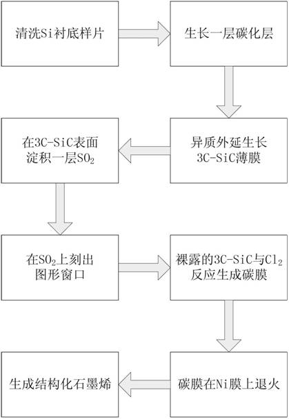
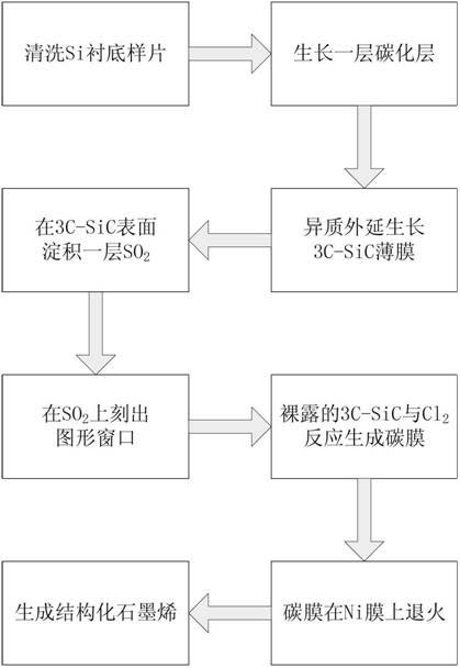
[0030] Step 1: Remove sample surface contamination.

[0031] Clean the surface of the 4-inch Si substrate substrate, that is, use NH 4 OH+H 2 o 2 Soak the sample in the reagent for 10 minutes, take it out and dry it to remove the organic residue on the surface of the sample; then use HCl+H 2 o 2 The reagent soaked the sample for 10 minutes, took it out and dried it to remove ionic contamination.

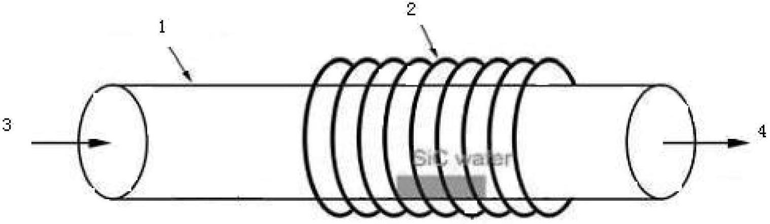
[0032] Step 2: Put the Si substrate substrate into the reaction chamber of the CVD system, and evacuate the reaction chamber to 10 -7 mbar level.

[0033] Step 3: growing the carbonized layer.

[0034] in H 2 In the case of protection, the temperature of the reaction chamber is raised to the carbonization temperature of 900 ° C, and then the flow rate of 30 sccm is introduced into the reaction chamber. 3 h 8 , grow a layer of carbonized layer on the Si substrate, the growth time is 10min.

[0035] Step 4: growing a 3C-SiC film on the carbide layer.

[0036] The temperature...

Embodiment 2

[0060] Step 1: Remove sample surface pollutants.

[0061] Clean the surface of the 8-inch Si substrate substrate, that is, use NH 4 OH+H 2 o 2 Soak the sample in the reagent for 10 minutes, take it out and dry it to remove the organic residue on the surface of the sample; then use HCl+H 2 o 2 The reagent soaked the sample for 10 minutes, took it out and dried it to remove ionic contamination.

[0062] Step 2: Same as Step 2 of Example 1.

[0063] Step 3: growing a carbonized layer.

[0064] in H 2 In the case of protection, the temperature of the reaction chamber is raised to the carbonization temperature of 1050 ° C, and then the flow rate of 30 sccm is introduced into the reaction chamber. 3 h 8 , grow a layer of carbonized layer on the Si substrate, the growth time is 7min.

[0065] Step 4: growing a 3C-SiC thin film on the carbide layer.

[0066] Rapidly raise the temperature of the reaction chamber to the growth temperature of 1200°C, and feed in SiH with flow r...

Embodiment 3

[0080] Step A: Clean the surface of the 12-inch Si substrate, that is, use NH 4 OH+H 2 o 2 Soak the sample in the reagent for 10 minutes, take it out and dry it to remove the organic residue on the surface of the sample; then use HCl+H 2 o 2 The reagent soaked the sample for 10 minutes, took it out and dried it to remove ionic contamination.

[0081] Step B: Same as Step 2 of Example 1.

[0082] Step C: In H 2 In the case of protection, the temperature of the reaction chamber is raised to the carbonization temperature of 1200 ° C, and then the flow rate of 30 sccm is introduced into the reaction chamber. 3 h 8 , for 5 min to grow a carbonized layer on the Si substrate.

[0083] Step D: Rapidly increase the temperature of the reaction chamber to the growth temperature of 1300° C., and feed SiH with flow rates of 30 sccm and 60 sccm respectively 4 and C 3 h 8 , carry out 3C-SiC film heteroepitaxial growth for 30min, and then in H 2 Gradually cool down to room temperat...


PUM


Abstract

The invention discloses a method for preparing structured graphene based on reaction of Cl2 and Ni film annealing, mainly aiming at solving the problems that the graphene prepared by the prior art is poor in continuity and uneven in the number of layers. The realization process of the method comprises the steps of: (1) leading a carbide layer to grow on a Si substrate for transition; (2) leading a 3C-SiC film to grow at the temperature of 1200-1300 DEG C; (3) depositing a layer of SiO2 on the surface of the 3C-SiC film, and carving a graphic window; (4) after the graphic window is formed, leading the exposed 3C-SiC to have reaction with Cl2 at the temperature of 700-1100 DEG C, and generating a carbon film; (5) then, putting the generated carbon film sample piece into a buffer hydrofluoric acid solution, and removing the SiO2 outside the window; (6) after that, depositing a layer of Ni film on another Si sample piece by electron beams; and (7) arranging the carbon film sample piece without SiO2 on the Ni film, and arranging in Ar gas; and carrying out annealing at 900-1100 DEG C for 15-30minutes, and generating the structured graphene at the position of the window of the carbon film. The structured graphene prepared by the invention is smooth in the surface, good in continuity and low in porosity, thus being used for making a microelectronic device.

Description

technical field [0001] The invention belongs to the technical field of microelectronics, and relates to a semiconductor thin film material and a preparation method thereof, specifically based on Ni film annealing and Cl 2 Reactive structured graphene preparation method. technical background [0002] Graphene appeared in the laboratory in 2004. At that time, two scientists, Andre Gem and Kostya Novoselov, from the University of Manchester in the United Kingdom discovered that they could obtain more and more graphene in a very simple way. thinner and thinner graphite flakes. They peeled off the graphite flakes from the graphite, then glued the two sides of the flakes to a special adhesive tape, and when the tape was torn off, the graphite flakes could be split in two. Repeatedly doing this, the flakes got thinner and thinner, and eventually, they got a flake made of just one layer of carbon atoms, which is graphene. Since then, new methods of preparing graphene have emerged...

Claims


Application Information

Patent Timeline
IPC IPC(8): C01B31/04H01L21/02C01B32/188
Inventor 郭辉张克基张凤祁张玉明雷天民邓鹏飞
Owner XIDIAN UNIV
Why Eureka
Try Eureka