Light detector of semiconductor quantum well

A semiconductor and quantum well technology, applied in the field of light wave detectors, can solve problems such as low efficiency and inability to achieve coupling, and achieve the effect of flexible design

Inactive Publication Date: 2012-10-03
FUDAN UNIV
View PDF1 Cites 11 Cited by
  • Summary
  • Abstract
  • Description
  • Claims
  • Application Information

AI Technical Summary

Problems solved by technology

[0003] In the disclosed technology of using a periodic metal hole structure as an optical coupling device for a quantum well photodetector, the main application is a layer of metal hole array structure, and the incident light is incident from one side of the metal layer. Although this coupling device is relatively The efficiency of oblique incidence and grating coupling in the early stage has been improved to some extent, but the efficiency is still low (absorption rate 7-10%, such as literature 7); at the same time, it is impossible to realize the combination of multiple surface plasmon modes and characteristic frequencies in semiconductors. coupling

Method used


Image

  • Light detector of semiconductor quantum well
  • Light detector of semiconductor quantum well
  • Light detector of semiconductor quantum well

Examples


Embodiment Construction

[0042] The present invention is further described below in conjunction with accompanying drawings and examples, but these accompanying drawings and examples do not constitute a limitation to the present invention.

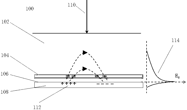
[0043] figure 1 It is a structural diagram of the present invention. Wherein, the incident light wave 110 is vertically incident from the side of the semiconductor material 102 and the quantum well layer 104, and is finally absorbed by the quantum well layer 104 to generate a surface plasmon wave 112, and its vertical electric field component 114 (E z ).

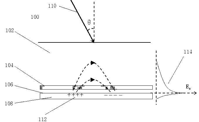
[0044] figure 2 It is a structural diagram of the present invention. where the incident light is at an angle of incidence Incident, it can detect one wavelength or two or more wavelengths at the same time.

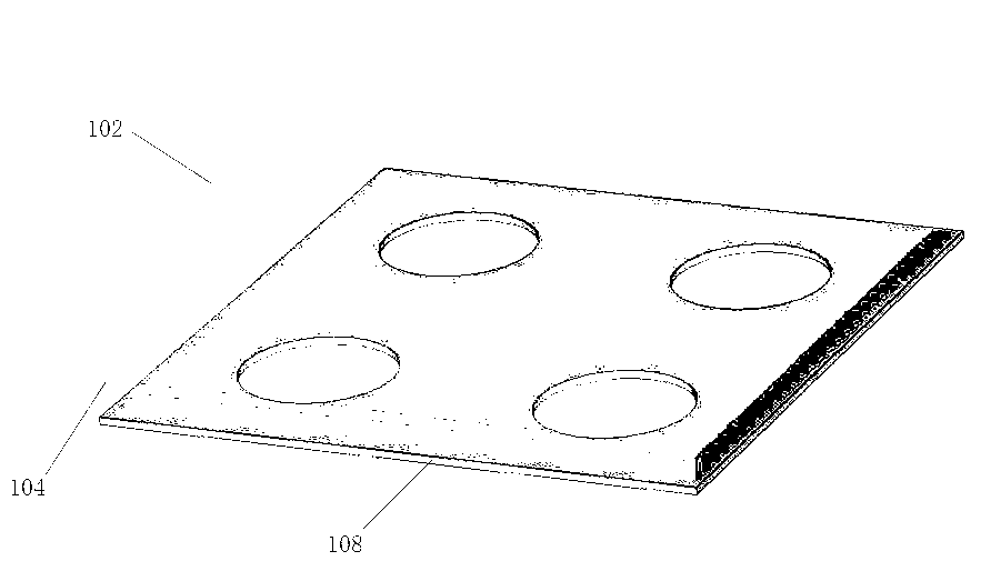
[0045] In the present invention, there are two kinds of metal layer periodic structures: one is a double-port periodic metal circular hole structure, that is, the thickness of the metal layer is equal ...


PUM


Abstract

The invention belongs to the technical field of light wave detectors, and particularly relates to a light detector of a semiconductor quantum well. The detector comprises a semiconductor layer, a quantum layer and a layer of a subwavelength periodic structured metal film. The quantum well at least comprises two energy levels and has a certain carrier concentration. Incident light wave with a certain spectrum width enters the semiconductor layer vertically or obliquely; the incident light wave stimulates the periodic structured metal film/a surface plasma of a quantum well interface; the surface plasma is absorbed by the semiconductor quantum well and an electronic subband transition process is generated; and the transited electrons form current signals under the externally applied bias voltage. According to the light detector of the semiconductor quantum well disclosed by the invention, the detection efficiency can be greatly improved.

Description

technical field [0001] The invention belongs to the technical field of light wave detectors, in particular to a semiconductor quantum well photodetection device. Background technique [0002] The use of quantum well structure devices for light detection is one of the main technologies for light detection in the mid- and far-infrared bands. However, on the one hand, the light wave absorption of the semiconductor quantum well structure is limited by the "polarization selection law" widely recognized in this field, that is, the quantum well can only absorb the light wave of the electric field component perpendicular to the quantum well plane, and in practical applications For direct vertically incident light wave absorption is extremely small, see Document 1 for example. Therefore, the actual device must be combined with complex processes such as oblique incidence (such as document 2), grating coupling (such as document 3) or etched groove structure (such as document 4). Thes...

Claims


Application Information

Patent Timeline
Patent Type & Authority Applications(China)
IPC IPC(8): H01L31/0352H01L31/101H01L31/0232
Inventor 安正华王恒亮
Owner FUDAN UNIV
Why Eureka
Try Eureka