Self-aligned-technology-based tri-polycrystal SOI (Silicon On Insulator), SiGe and HBT (Heterojunction Bipolar Transistor) integrated device and preparation method thereof
A self-alignment process and integrated device technology, which is applied in semiconductor/solid-state device manufacturing, semiconductor devices, electrical components, etc., and can solve the problems of low mechanical strength, high cost, incompatibility with wide application and development, etc.
- Summary
- Abstract
- Description
- Claims
- Application Information
AI Technical Summary
Problems solved by technology
Method used
Image
Examples
Embodiment 1
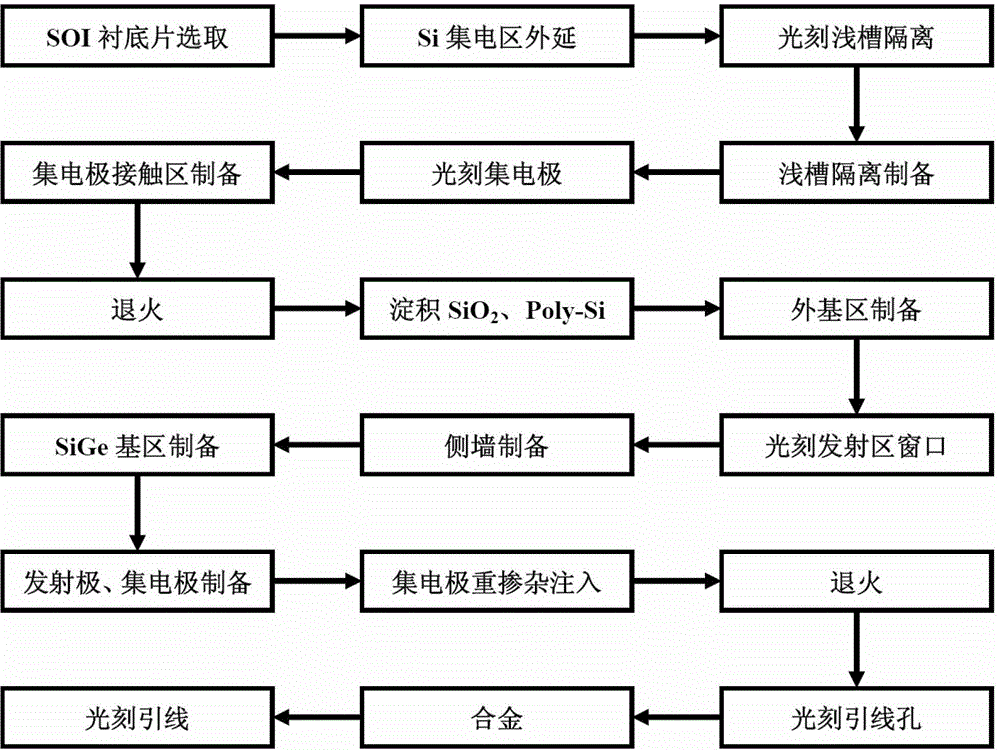
[0080] Embodiment 1: A self-aligned process is used to prepare a three-polycrystalline SOI SiGe HBT integrated device and a circuit method with a base thickness of 20 nm. The specific steps are as follows:
[0081] Step 1, epitaxial growth, as shown in Figure 2(a).
[0082] (1a) Select SOI substrate, the support material 1 of the substrate is Si, and the intermediate layer 2 is SiO 2 , The thickness is 150nm, the upper material 3 is doped with a concentration of 1×10 16 cm -3 N-type Si with a thickness of 100nm;
[0083] (1b) Using chemical vapor deposition (CVD) method, at 600℃, grow a layer of N-type epitaxial Si layer 4 with a thickness of 50nm on the upper layer of Si material as a collector area, the doping concentration of this layer is 1 ×10 16 cm -3 .
[0084] Step 2, shallow trench isolation preparation, as shown in Figure 2 (b) and (c).
[0085] (2a) Using chemical vapor deposition (CVD) method, at 600℃, grow a layer of SiO with a thickness of 300nm on the surface of the epit...
Embodiment 2
[0116] Embodiment 2: Using a self-aligned process to prepare a three-polycrystalline SOI SiGe HBT integrated device and a circuit method with a base thickness of 40 nm, the specific steps are as follows:
[0117] Step 1, epitaxial growth, as shown in Figure 2(a).
[0118] (1a) Select an SOI substrate, the lower support material 1 of the substrate is Si, and the intermediate layer 2 is SiO 2 , The thickness is 300nm, the upper material 3 is doped with a concentration of 5×10 16 cm -3 N-type Si with a thickness of 120nm;
[0119] (1b) Using the chemical vapor deposition (CVD) method, at 700℃, grow a layer of N-type epitaxial Si layer 4 with a thickness of 80nm on the upper Si material as a collector area, the doping concentration of this layer is 5 ×10 16 cm -3 .
[0120] Step 2, shallow trench isolation preparation, as shown in Figure 2 (b) and (c).
[0121] (2a) Using chemical vapor deposition (CVD) method, at 700℃, grow a layer of SiO with a thickness of 400nm on the surface of the ep...
Embodiment 3
[0152] Embodiment 3: Using a self-aligned process to prepare a three-polycrystalline SOI SiGe HBT integrated device and circuit method with a base thickness of 60 nm, the specific steps are as follows:
[0153] Step 1, epitaxial growth, as shown in Figure 2(a).
[0154] (1a) Select an SOI substrate, the lower support material 1 of the substrate is Si, and the intermediate layer 2 is SiO 2 , The thickness is 400nm, and the upper material 3 is doped with a concentration of 1×10 17 cm -3 N-type Si with a thickness of 150nm;
[0155] (1b) Using the chemical vapor deposition (CVD) method, at 750℃, grow a layer of N-type epitaxial Si layer 4 with a thickness of 100nm on the upper Si material as a collector area, the doping concentration of this layer is 1 ×10 17 cm -3 .
[0156] Step 2, shallow trench isolation preparation, as shown in Figure 2 (b) and (c).
[0157] (2a) Using chemical vapor deposition (CVD), at 800℃, grow a layer of SiO with a thickness of 500nm on the surface of the epitax...
PUM
| Property | Measurement | Unit |
|---|---|---|
| Thickness | aaaaa | aaaaa |
| Thickness | aaaaa | aaaaa |
| Thickness | aaaaa | aaaaa |
Abstract
Description
Claims
Application Information


