High-speed phase splitting circuit with band spreading function

A frequency band expansion and functional technology, applied in the field of high-speed phase splitting circuit, can solve the problems of lossy integrator output common-mode voltage deviation, post-stage circuit DC offset, phase splitting amplifier output differential signal DC deviation, etc., to improve work Frequency, the effect of expanding the operating bandwidth

Inactive Publication Date: 2012-10-10
FUJIAN EOCHIP SEMICON CO LTD
View PDF4 Cites 12 Cited by
  • Summary
  • Abstract
  • Description
  • Claims
  • Application Information

AI Technical Summary

Problems solved by technology

However, this solution has the following disadvantages: First, the phase splitting circuit does not have the function of frequency extension, and cannot improve the operating frequency of the entire preamplifier
However, due to the existence of random mismatch in the processing process, the compensation resistor cannot be exactly equal to the linear resistance of the lossy integrator, which will cause the output common-mode voltage of the lossy integrator to deviate, and the output differential signal of the phase-splitting amplifier will appear significantly The DC deviation will cause unnecessary DC offset to the subsequent stage circuit, resulting in misjudgment of the optical receiving module

Method used


Image

  • High-speed phase splitting circuit with band spreading function
  • High-speed phase splitting circuit with band spreading function
  • High-speed phase splitting circuit with band spreading function

Examples


specific Embodiment approach 1

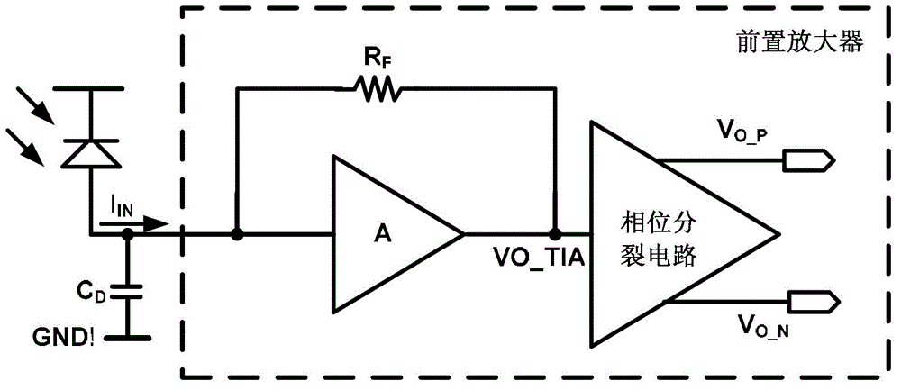
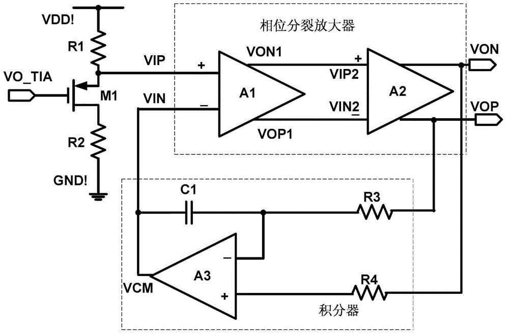
[0039] Specific implementation mode one: the following combination figure 2 Describe this embodiment, the high-speed phase splitting circuit with frequency band extension function described in this embodiment, it includes the first PMOS transistor M1, resistor R1, resistor R2, phase splitting amplifier and integrator,

[0040] The phase splitting amplifier is composed of the first amplifier A1 and the second amplifier A2 cascaded,

[0041] The integrator is composed of a third amplifier A3, a resistor R3, a resistor R4 and a capacitor C1,

[0042] One end of the resistor R1 is connected to the power supply VDD! , the other end of the resistor R1 is simultaneously connected to the source of the first PMOS transistor M1 and the non-inverting input terminal VIP of the first amplifier A1, the gate of the first PMOS transistor M1 is used as the receiving end of the transimpedance amplifier output signal VO_TIA, and the first PMOS transistor M1 The drain is connected to one end o...

specific Embodiment approach 2

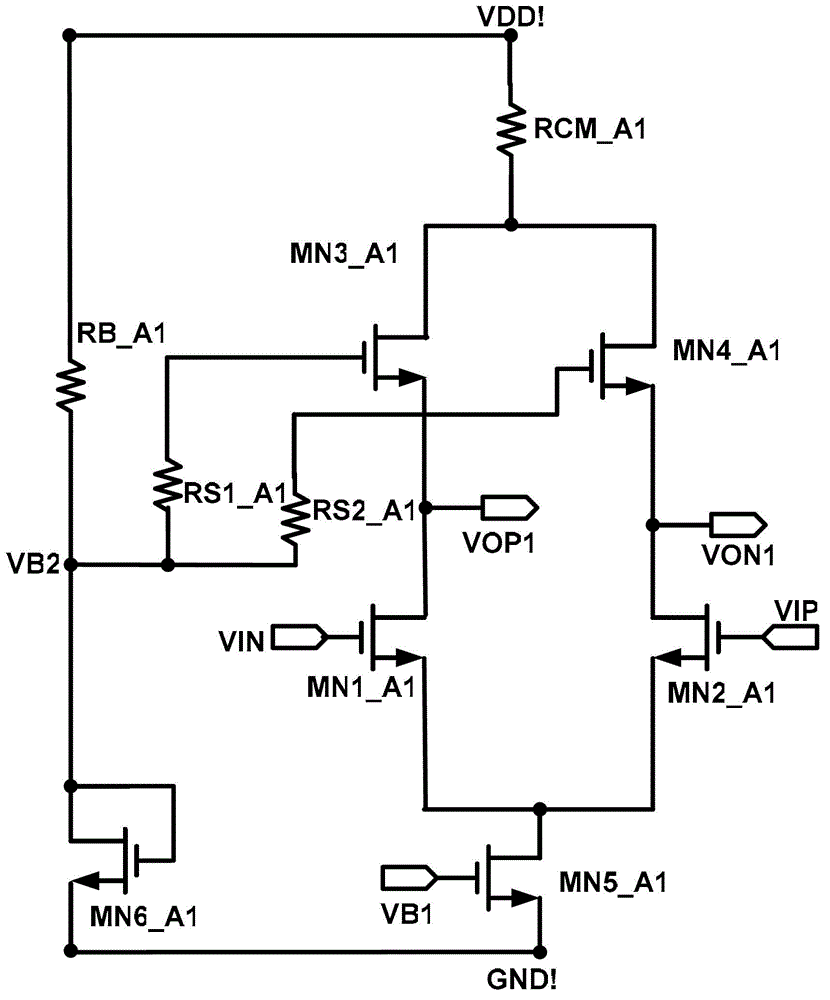
[0053] Specific implementation mode two: the following combination image 3 Describe this embodiment. This embodiment is a further description of Embodiment 1. The first amplifier A1 includes a first NMOS transistor MN1_A1, a second NMOS transistor MN2_A1, a third NMOS transistor MN3_A1, a fourth NMOS transistor MN4_A1, and a fifth NMOS transistor. MN5_A1, sixth NMOS transistor MN6_A1, resistor RB_A1, resistor RS1_A1, resistor RS2_A1 and resistor RCM_A1,

[0054] One end of the resistor RB_A1 is connected to the power supply VDD! , the other end of the resistor RB_A1 is connected to the common terminal of the gate of the sixth NMOS transistor MN6_A1 and its drain, and the source of the sixth NMOS transistor MN6_A1 is connected to GND! ;

[0055] One end of the resistor RCM_A1 is connected to the power supply VDD! , the other end of the resistor RCM_A1 is connected to the drain common end of the third NMOS transistor MN3_A1 and the fourth NMOS transistor MN4_A1;

[0056] Th...

specific Embodiment approach 3

[0066] Specific implementation mode three: the following combination Figure 4 This embodiment is described. This embodiment is a further description of Embodiment 1 or 2. The second amplifier A2 includes a seventh NMOS transistor MN1_A2, an eighth NMOS transistor MN2_A2, a ninth NMOS transistor MN3_A2, a second PMOS transistor MP1_A2, a third PMOS transistor MP2_A2, resistor RL1_A2, resistor RL2_A2, resistor RC_A2, capacitor CL1_A2 and capacitor CL2_A2,

[0067] One end of the resistor RC_A2 is connected to the power supply VDD! , the other end of the resistor RC_A2 is connected to the source common terminals of the second PMOS transistor MP1_A2 and the third PMOS transistor MP2_A2,

[0068] The capacitor CL1_A2 is connected between the source and the gate of the second PMOS transistor MP1_A2, the resistor RL1_A2 is connected between the drain and the gate of the second PMOS transistor MP1_A2,

[0069] The capacitor CL2_A2 is connected between the source and the gate of the t...


PUM


Abstract

The invention discloses a high-speed phase splitting circuit with a band spreading function, belongs to the field of communication circuits, and aims to solve the problem of limitation of the bandwidth of a trans-impedance amplifier in the conventional phase splitting circuit on the working frequency of a pre-amplifier. The high-speed phase splitting circuit with the band spreading function comprises a first P-channel metal oxide semiconductor (PMOS) transistor M1, a resistor R1, a resistor R2, a phase splitting amplifier and an integrator, wherein the phase splitting amplifier is formed by cascading a first amplifier A1 and a second amplifier A2; the integrator consists of a third amplifier A3, a resistor R3, a resistor R4 and a capacitor C1; a source of the first PMOS transistor M1 is connected with a power supply through the resistor R1 and also connected with a non-inverting input end of the first amplifier A1, and a drain of the first PMOS transistor M1 is grounded through the resistor R2; two output ends of the second amplifier A2 are respectively connected with two input ends of the integrator; and the output end of the integrator is connected with an inverting input end of the first amplifier A1.

Description

technical field [0001] The invention relates to a high-speed phase splitting circuit for optical fiber preamplifiers. The phase splitting circuit uses a phase splitting amplifier with a frequency band extension function to increase the operating frequency of the preamplifier. Background technique [0002] Optical fiber communication uses light as the information carrier and optical fiber as the transmission medium. It has the advantages of high bandwidth, low loss, and small external electromagnetic interference. It has become the main form of network communication. The optical transceiver module is the core device of the optical fiber access network, mainly composed of two parts: the receiving module and the transmitting module. The transmitter module is mainly composed of a laser drive circuit and a laser diode (LD). The laser diode converts the electrical signal sent by the user into an optical signal and emits it. The drive circuit provides the drive current for the lase...

Claims


Application Information

Patent Timeline
Patent Type & Authority Applications(China)
IPC IPC(8): H03F1/42
Inventor 李景虎张远燚李博阳
Owner FUJIAN EOCHIP SEMICON CO LTD
Why Eureka
Try Eureka