Semiconductor ceramic and multilayer semiconductor ceramic capacitor

A technology of ceramic capacitors and semiconductors, applied in the direction of multilayer capacitors, capacitors, fixed capacitors, etc., can solve the problem of lowering the dielectric constant, and achieve the effect of large-capacity multilayer semiconductor ceramic capacitors

Inactive Publication Date: 2012-10-17
TDK CORPARATION
View PDF8 Cites 0 Cited by
  • Summary
  • Abstract
  • Description
  • Claims
  • Application Information

AI Technical Summary

Problems solved by technology

However, when the conductivity of semiconducting ceramics is too high, it is necessary to thicken the insulating coating layer in order to maintain the insulation resistance, but there is a problem that the apparent relative permittivity decreases when the thickness is increased.

Method used


Image

  • Semiconductor ceramic and multilayer semiconductor ceramic capacitor
  • Semiconductor ceramic and multilayer semiconductor ceramic capacitor
  • Semiconductor ceramic and multilayer semiconductor ceramic capacitor

Examples


Embodiment 1~14

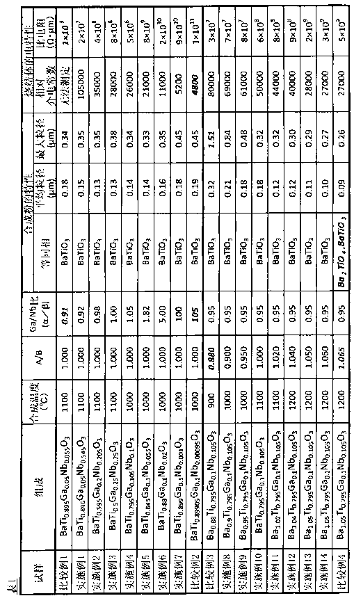
[0067] (Examples 1-14, Comparative Examples 1-4)

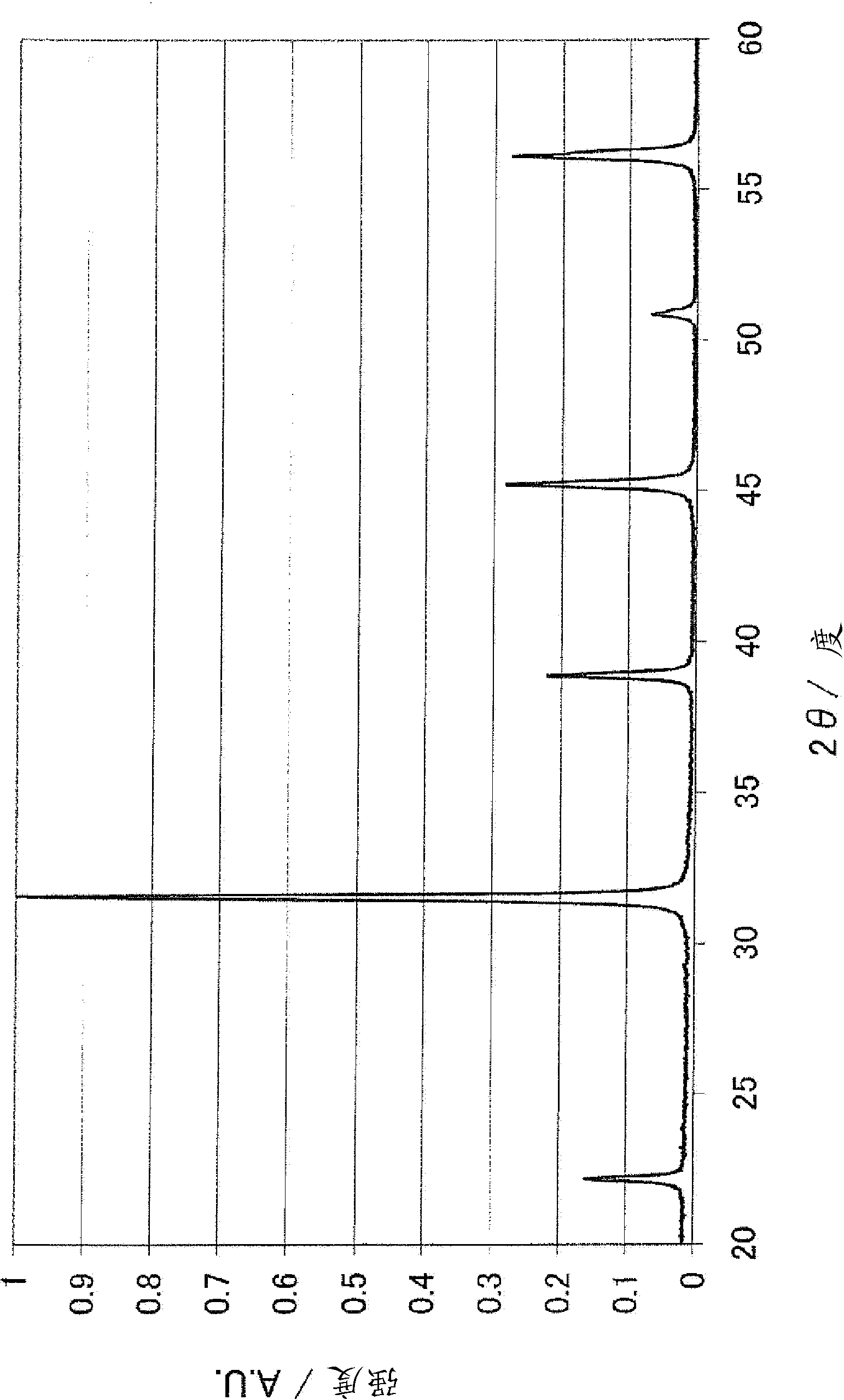
[0068] First, prepare BaCO as a raw material powder 3 (specific surface area: 25m 2 / g), TiO 2 (specific surface area: 50m 2 / g), Ga 2 o 3 (specific surface area: 10m 2 / g) and Nb 2 o 5 (specific surface area: 10m 2 / g), weighed according to the composition shown in Table 1.

[0069]

[0070]Next, the weighed raw material powder is mixed with water and a dispersant by a ball mill to prepare a raw material mixture. The obtained mixed powder was treated under the following heat treatment conditions to produce barium titanate-based semiconductor fine particles.

[0071] The heat treatment conditions were heating rate: 200°C / hour, holding temperature: the temperature shown in Table 1, temperature holding time: 2 hours, cooling rate: 200°C / hour, in the air.

[0072] From the above, barium titanate-based semiconductor fine particles capable of contributing to thinning of the dielectric layer can be obtained.

[0073] ...

Embodiment 15

[0090] SiO was added in such a way that it was 0.5 mol relative to 100 mol of Ti element of the synthetic powder produced in Example 10. 2 , put into a ball mill together with a dispersant, fully wet-mix in the ball mill, evaporate and dry, and then perform a heat treatment at 500° C. for about 3 hours in an air atmosphere to produce a heat-treated powder.

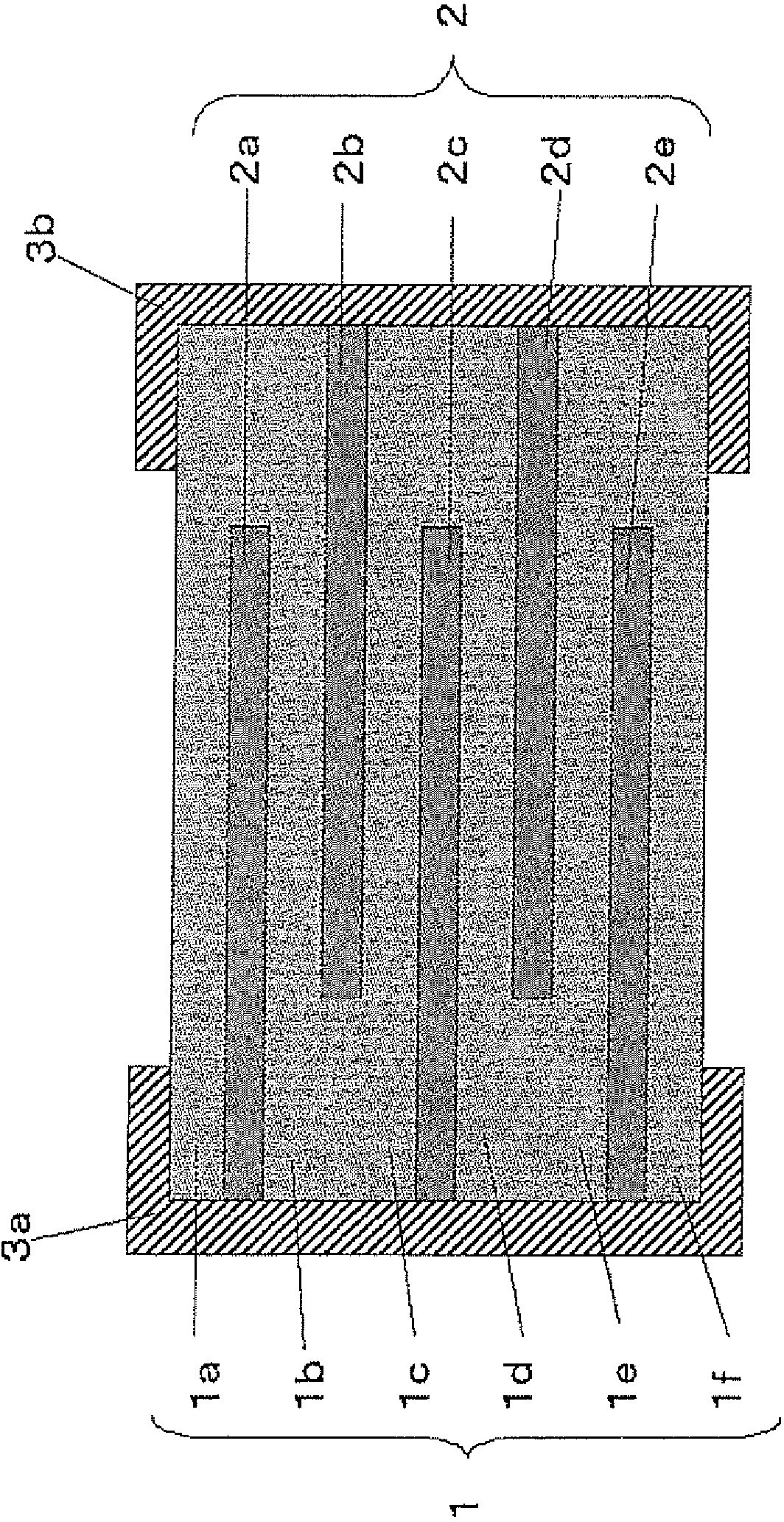
[0091] Next, 0.3 mol of Mn was added to 100 mol of Ti element in the synthetic powder, and an appropriate amount of an organic solvent such as alcohol fuel or a dispersant was added. Then, it is poured into a ball mill together with water, fully wet-mixed in the ball mill, and then an appropriate amount of an organic binder or plasticizer is added, and wet-mixed for a long enough time to obtain a ceramic slurry.

[0092] Next, the ceramic slurry was subjected to forming processing using a forming processing method such as a doctor blade method, so that the thickness after drying was 1 μm, and a ceramic green sheet was prod...


PUM

PropertyMeasurementUnit
particle sizeaaaaaaaaaa
thicknessaaaaaaaaaa
particle sizeaaaaaaaaaa

Abstract

The present invention relates to a semiconductor ceramic and to a multilayer semiconductor ceramic capacitor. More precisely, the present invention relates to a BaTiO3 based grain boundary insulating type semiconductor ceramic and to a multilayer semiconductor ceramic capacitor using thereof. A purpose of the present invention is to provide a multilayer semiconductor ceramic capacitor, which makes coexistence of a high dielectric property and a high insulating resistance of a semiconductor ceramic possible by improving insulating property of the semiconductor ceramic component. In order to achieve such object, BaTiO3 based semiconductor ceramic of the invention is expressed by BaA(Ti1-[alpha]-[beta]Ga[alpha]Nb[beta])BO3, wherein A / B mole ratio is within a range of 0.900 or more to 1.060 or less and [alpha] / [beta] mole ratio is within a range of 0.92 or more to 100 or less.

Description

technical field [0001] The present invention relates to semiconducting ceramics and laminated semiconducting ceramic capacitors, more particularly to BaTiO 3 It is a grain boundary insulation type semiconducting ceramic and a multilayer semiconducting ceramic capacitor using it. Background technique [0002] With the development of electronic technology in recent years, the miniaturization of electronic components is rapidly advancing. Furthermore, in the field of multilayer ceramic capacitors, the demand for miniaturization and increase in capacity is increasing, so the development of ceramic materials with high relative permittivity and the thinning and multilayering of dielectric ceramic layers are being promoted. [0003] For example, the general formula is proposed in the Japanese Patent Application No. 11-302072 communique: {Ba 1-x-y Ca x Re y O} m TiO 2 +αMgO+βMnO (Re is a rare earth element selected from Y, Gd, Tb, Dy, Ho, Er and Yb, α, β, m, x and y are each 0...

Claims


Application Information

Patent Timeline
Patent Type & Authority Applications(China)
IPC IPC(8): C04B35/468H01G4/12H01G4/30
CPCC04B2235/81C04B2235/3418C04B2235/5409C04B2235/5445C04B35/4682C04B2235/79H01G4/1227C04B2235/6567C04B2235/3286C04B2235/6025C04B2235/3251C04B2235/6565C04B2235/6562C04B2235/5436C04B35/468H01G4/12
Inventor 石井辰也增田健一郎日高重和夏井秀定塚田岳夫
Owner TDK CORPARATION
Why Eureka
Try Eureka