Array waveguide grating structure based on PLC (programmable logic controller) technique and manufacturing method thereof

An arrayed waveguide grating technology and a manufacturing method, which are applied in the directions of light guides, optics, optical components, etc., can solve the problems of increased polarization-related loss of devices, large differences in thermal expansion coefficients, affecting product performance, etc., so as to reduce polarization-related losses and reduce Stress effect, good product performance

Inactive Publication Date: 2012-10-17
无锡思力康光子科技有限公司
View PDF3 Cites 11 Cited by
  • Summary
  • Abstract
  • Description
  • Claims
  • Application Information

AI Technical Summary

Problems solved by technology

Although the waveguide film obtained by the thermal oxidation method has good density and uniformity, due to the slow film formation speed of thermal oxidation, the growth cycle is long, and the growth cost is high; and its thermal expansion coefficient with the silicon substrate and the upper cladding material The difference is large, and the stress generated between the layers is large, which makes the polarization-dependent loss of the device larger, which greatly affects the product performance
[0007] In the process of realizing the present invention, the inventor found that there are at least defects such as long growth cycle, high cost and poor product performance in the prior art

Method used


Image

  • Array waveguide grating structure based on PLC (programmable logic controller) technique and manufacturing method thereof
  • Array waveguide grating structure based on PLC (programmable logic controller) technique and manufacturing method thereof

Examples


Embodiment Construction

[0031] The preferred embodiments of the present invention will be described below in conjunction with the accompanying drawings. It should be understood that the preferred embodiments described here are only used to illustrate and explain the present invention, and are not intended to limit the present invention.

[0032] Example of Fabrication Method of Arrayed Waveguide Grating Structure

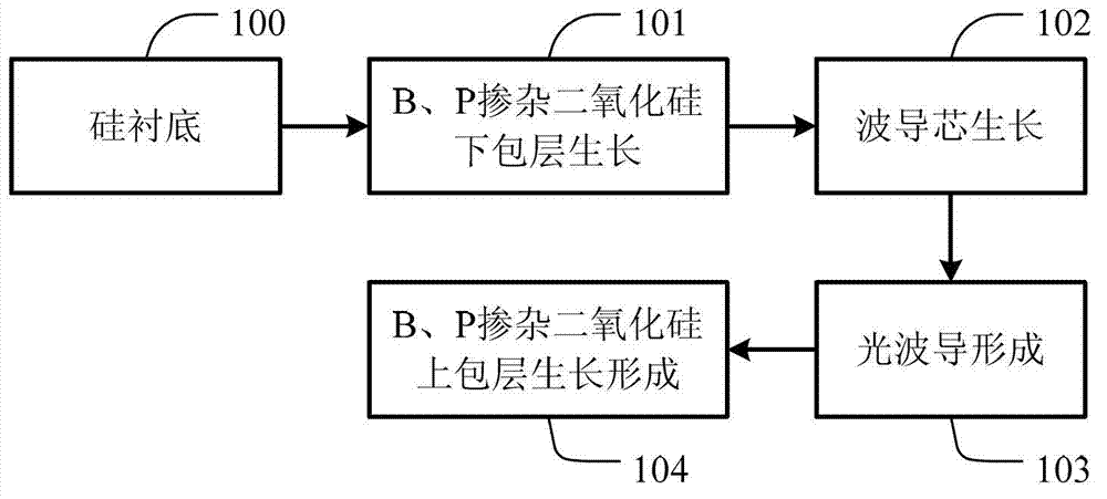
[0033] According to an embodiment of the present invention, a method for fabricating an arrayed waveguide grating structure based on PLC technology is provided. like figure 2 As shown, this embodiment includes:

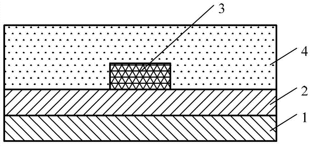
[0034] Step 100: choose silicon as the substrate, i.e. silicon substrate;

[0035] Step 101: On the silicon substrate selected in step 100, a PECVD process is used to deposit and grow a doped B and P silicon dioxide layer as a lower cladding layer;

[0036] Step 102: growing a waveguide core layer on the lower cladding layer obtained in step 101;

[0037] Step 103: On the w...


PUM


Abstract

The invention discloses an array waveguide grating structure based on a PLC (programmable logic controller) technique and a manufacturing method thereof. The manufacturing method comprises the following steps of: selecting a substrate, depositing and growing a B and P doped silica layer as a lower coating layer on the selected substrate by adopting a PECVD (plasma enhanced chemical vapor deposition) process; growing a waveguide core layer on the lower coating layer; preserving a waveguide core in a preset shape on the waveguide core layer, and corroding to remove the part except the waveguide core in the preset shape and to remain the waveguide core in the preset shape; and growing a B and P highly doped silica layer capable of completely covering the lower coating layer and the waveguide core as an upper coating layer on the lower coating layer and the waveguide core, so that the needed array waveguide grating structure based on the PLC technique is manufactured. By using the array waveguide grating structure based on the PLC technique and the manufacturing method thereof, which are provided by the invention, the defects of long growth period, high cost, bad product performance and the like in the prior art can be overcome, so as to realize the advantages of short growth period, low cost and good product performance.

Description

technical field [0001] The invention relates to the technical field of semiconductors, in particular to an arrayed waveguide grating structure based on PLC technology and a manufacturing method thereof. Background technique [0002] The optical devices developed based on the Planar Lightwave Circuit (PLC) technology play an important role in the networking of optical networks. The Waveguide Division Multiplexing (WDM for short) system is currently the most common optical layer networking technology, which implements multiplex signal transmission through a multiplexer / demultiplexer. Arrayed Wave-guide Grating (AWG for short) manufactured by PLC technology is an important device for wavelength division multiplexing, which is a supporting technology used in optical networks. [0003] Arrayed waveguide gratings were one of the first components to commercialize PLC technology. It is a wavelength division multiplexing device based on the principle of interference. The integrated...

Claims


Application Information

Patent Timeline
Patent Type & Authority Applications(China)
IPC IPC(8): G02B6/132G02B6/124
Inventor 宋齐望孙麦可
Owner 无锡思力康光子科技有限公司
Why Eureka
Try Eureka