Proximity field exposure device and method

An exposure device and exposure method technology, applied in the field of photolithography, can solve the problems of high cost, cannot replace Aligner, low yield, etc., and achieve the effects of low cost, fast movement speed, and short stabilization time

Active Publication Date: 2012-10-17
SHANGHAI MICRO ELECTRONICS EQUIP (GRP) CO LTD
View PDF8 Cites 10 Cited by
  • Summary
  • Abstract
  • Description
  • Claims
  • Application Information

AI Technical Summary

Problems solved by technology

However, because the projection lithography machine has splicing problems between fields, and the yield is lower than that of the automatic Aligner, and more importantly, the cost of the projection l

Method used


Image

  • Proximity field exposure device and method
  • Proximity field exposure device and method
  • Proximity field exposure device and method

Examples


Embodiment Construction

[0036] In the following, preferred embodiments according to the present invention will be described in detail with reference to the accompanying drawings. For the convenience of describing and highlighting the present invention, relevant components existing in the prior art are omitted from the drawings, and the description of these known components will be omitted.

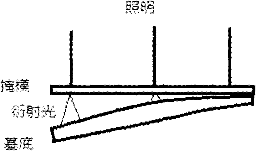
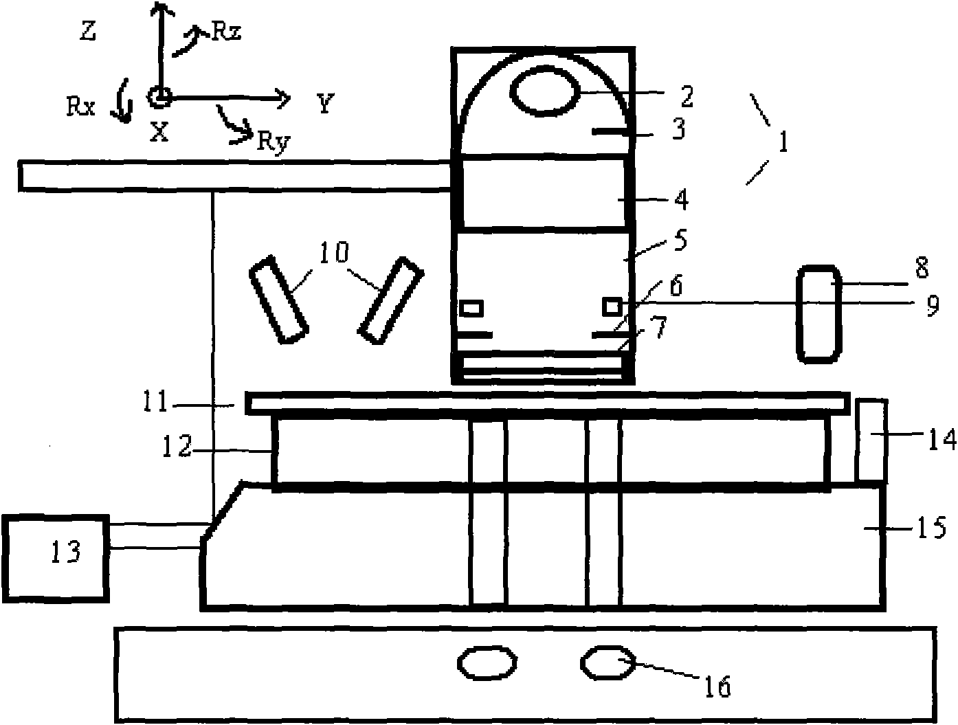
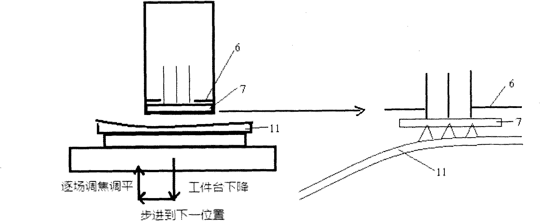
[0037] figure 2 Shown is a schematic structural view of the exposure device according to the present invention. The exposure device according to the present invention includes an illumination subsystem 1 , a workpiece table 15 , a position measurement subsystem 13 , a focusing and leveling subsystem 10 , an alignment subsystem 8 and the like. The lighting subsystem 1 includes a light source 2 and a homogenizer 4. The light source 2 can be a mercury lamp, which provides uniform parallel light illumination for the mask 7 after being converged by a concave mirror and homogenized by the homogenizer 4. The mask 7 i...


PUM


Abstract

A proximity field exposure device comprises an illumination subsystem, a working table, a position measurement subsystem, a focusing and leveling subsystem and an aligning subsystem. Uniform parallel rays which are emitted from the illumination subsystem are incident on a mask on a reticle stage. The proximity field exposure device is characterized in that a field substrate of the exposure device is small; and the working table has six degrees of freedom, namely XYZRxRyRz, wherein long-range motion can be carried out in the XY direction and small-range adjustment can be conducted in the ZRxRyRz direction. Before exposure, surface shape measurement and alignment are firstly carried out on the substrate. During the exposure process, according to the surface shape date of the substrate and the alignment data, the illumination system is turned on for field exposure in dependence on exposure formulation.

Description

technical field [0001] The invention relates to the field of photolithography, in particular to a proximity type field-by-field exposure device and method. Background technique [0002] LED (Light Emitting Diode), that is, light emitting diode, is a semiconductor solid light emitting device. LED can be divided into high-power LED and low-power LED according to power, and can be divided into high-brightness LED (HB-LED) and low-brightness LED according to brightness. At present, most of the substrates for LED production are sapphire substrates (Al203). Due to the physical characteristics and processing technology of sapphire, the flatness of sapphire substrates cannot reach the um level like silicon substrates. According to SEMI standards, the flatness of 4-inch sapphire substrates The worst flatness is 40um, and the worst flatness of 6-inch sapphire substrate is 60um. [0003] The most commonly used lithography machine in LED exposure is Aligner, which uses a large mask cl...

Claims


Application Information

Patent Timeline
IPC IPC(8): G03F7/20G03F9/00
Inventor 张俊陈勇辉
Owner SHANGHAI MICRO ELECTRONICS EQUIP (GRP) CO LTD
Why Eureka
Try Eureka