Method for forming semiconductor structure

A semiconductor and plasma technology, which is applied in semiconductor/solid-state device manufacturing, electrical components, circuits, etc., can solve the problems of thinning mask layer, stronger physical bombardment of high-energy ions, and slow gas exchange, etc. The effect of eclipse selection ratio

Active Publication Date: 2012-10-17
ADVANCED MICRO FAB EQUIP INC CHINA
View PDF8 Cites 31 Cited by
  • Summary
  • Abstract
  • Description
  • Claims
  • Application Information

AI Technical Summary

Problems solved by technology

[0006] However, it is found in actual production that as the size of the device shrinks, the size of the through hole also shrinks, especially when the existing plasma etching process is used to form a through hole with a high aspect ratio. As the etching progresses, the gas exchange in the through hole becomes slower and slower, so it is necessary to strengthen the bias power to enhance the gas exchange and the reaction rate in the through hole,

Method used


Image

  • Method for forming semiconductor structure
  • Method for forming semiconductor structure
  • Method for forming semiconductor structure

Examples


no. 2 example

[0071] refer to Figure 10 , Figure 10 It is a schematic flowchart of a method for forming a semiconductor structure according to the second embodiment of the present invention, including:

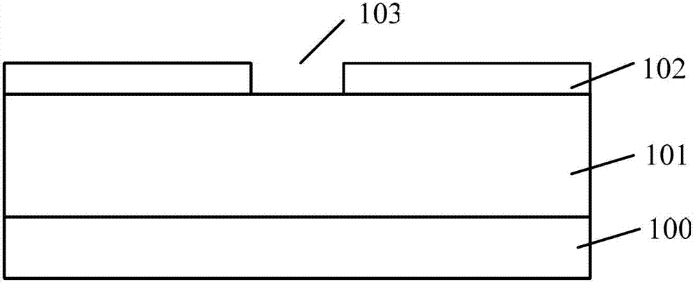
[0072] Step S31, providing a substrate, and forming a dielectric layer on the substrate;

[0073] Step S32, forming a mask layer on the dielectric layer, the mask layer having openings exposing the surface of the dielectric layer;

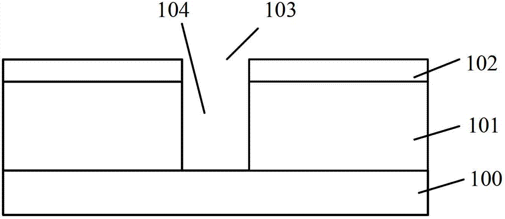
[0074] Step S33, using the mask layer as a mask to perform plasma etching on the dielectric layer, the radio frequency power source outputs radio frequency power in a continuous manner, the bias power source outputs bias power in a pulsed manner, and the bias The first duty cycle of the output pulse of the power source is continuously reduced. When the bias power source is turned on, a part of the dielectric layer is etched to form an etching hole. When the bias power source is turned off, a polymerization layer is formed on the surface of the mask layer. o...

no. 3 example

[0094] refer to Figure 17 , Figure 17 It is a schematic flowchart of a method for forming a semiconductor structure according to the third embodiment of the present invention, including:

[0095] Step S41, providing a base, and forming a dielectric layer on the base;

[0096] Step S42, forming a mask layer on the dielectric layer, the mask layer having openings exposing the surface of the dielectric layer;

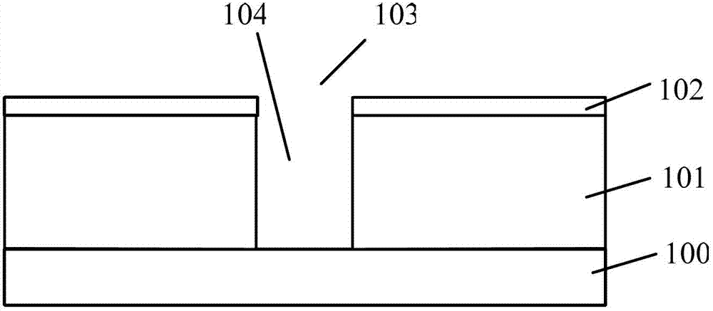
[0097] Step S43, using the mask layer as a mask to perform plasma etching on the dielectric layer, the radio frequency power source and the bias power source both output radio frequency power in a pulsed manner, and the radio frequency power source and the bias power source pulse The output frequencies are equal, the second duty cycle of the output pulse of the RF power source remains unchanged, the first duty cycle of the output pulse of the bias power source is equal to the second duty cycle of the output pulse of the RF power source, when the RF power source is turn...

no. 4 example

[0118] refer to Figure 23 , Figure 23 It is a schematic flowchart of a method for forming a semiconductor structure according to a fourth embodiment of the present invention, including:

[0119] Step S51, providing a substrate, and forming a dielectric layer on the substrate;

[0120] Step S52, forming a mask layer on the dielectric layer, the mask layer having openings exposing the surface of the dielectric layer;

[0121] Step S53, using the mask layer as a mask to perform plasma etching on the dielectric layer, the radio frequency power source and the bias power source both output radio frequency power in a pulsed manner, and the radio frequency power source and the bias power source pulse The output frequencies are equal, the second duty cycle of the output pulse of the RF power source remains unchanged, the first duty cycle of the output pulse of the bias power source is smaller than the second duty cycle of the output pulse of the RF power source, when the RF power s...


PUM


Abstract

The invention discloses a method for forming a semiconductor structure, which comprises the following steps: providing a substrate and forming a dielectric layer on the substrate; forming a mask layer provided with an opening for exposing the surface of the dielectric layer on the dielectric layer; carrying out a plasma etching on the dielectric layer by taking the mask layer as a mask, wherein a bias power source outputs a bias power in pulse mode, when the bias power resource is switched on, etching part of the dielectric layer to form an etch-hole, when the bias power resource is switched off, forming a polymer on the surface of the mask layer, repeating the process of switching on the bias power resource and switching off the bias power resource till a through hole is formed. When forming the through hole, the etching step and the polymer forming step are repeated so that the polymer can keep a certain thickness, therefore, in the entire etching process, the mask layer is protected from damaging or the damage rate is reduced, and the etching ratio of the dielectric layer relative to the mask layer is increased.

Description

technical field [0001] The invention relates to the field of semiconductor manufacturing, in particular to a method for forming a semiconductor structure. Background technique [0002] With the development of integrated circuits to sub-micron dimensions, the density of devices and the complexity of processes are increasing, and strict control of the process becomes more important. Among them, the through hole is used as the interconnection between the multilayer metal layers and the connection channel between the active area of ​​the device and the external circuit. Due to its important role in the composition of the device structure, the formation process of the through hole has always been a technical skill in the art. personnel's attention. [0003] Figure 1~Figure 3 It is a structural schematic diagram of the existing through-hole forming process. [0004] refer to figure 1 , providing a semiconductor substrate 100, forming a dielectric layer 101 on the semiconducto...

Claims


Application Information

Patent Timeline
IPC IPC(8): H01L21/3065H01L21/768
Inventor 王兆祥梁洁邱达燕
Owner ADVANCED MICRO FAB EQUIP INC CHINA
Why Eureka
Try Eureka