Method for forming semiconductor structure

A semiconductor and stacked structure technology, applied in semiconductor/solid-state device manufacturing, electrical components, circuits, etc., can solve the problems of shrinkage, achieve good sidewall morphology, improve efficiency, and reduce etching time

Active Publication Date: 2012-10-17
ADVANCED MICRO FAB EQUIP INC CHINA
View PDF13 Cites 30 Cited by
  • Summary
  • Abstract
  • Description
  • Claims
  • Application Information

AI Technical Summary

Problems solved by technology

[0006] However, in actual production, it is found that with the reduction of the size of the device, the size of the via hole is also reduced, especially when the existing plasma etching process is used to form a via hole with a high aspect ratio. Make the side wall of the formed through hole 104 have such as image 3 The wavy defect

Method used


Image

  • Method for forming semiconductor structure
  • Method for forming semiconductor structure
  • Method for forming semiconductor structure

Examples


no. 2 example

[0067] refer to Figure 9 , Figure 9 It is a schematic flowchart of a method for forming a semiconductor structure according to the second embodiment of the present invention, including:

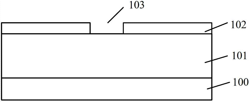
[0068] Step S31, providing a substrate, forming a multi-layer stack structure in which silicon nitride layers and silicon oxide layers are alternately distributed on the substrate, forming a mask layer on the surface of the stack structure, and the mask layer has a surface that exposes the stack structure surface open mouth

[0069] Step S32, performing plasma etching on the stacked structure, the bias power source outputs bias power in a pulsed manner, the plasma etching is a plasma etching with a continuously decreasing duty cycle, when the bias power When the source is turned on, part of the stacked structure is etched to form an etching hole; when the bias power source is turned off, a polymer is formed on the sidewall and bottom of the formed etching hole, and the bias power source i...

no. 3 example

[0087] refer to Figure 14 , Figure 14 It is a schematic flowchart of a method for forming a semiconductor structure according to the third embodiment of the present invention, including:

[0088] Step S41, providing a substrate, forming a multi-layer stack structure in which silicon nitride layers and silicon oxide layers are alternately distributed on the substrate, forming a mask layer on the surface of the stack structure, and the mask layer has a surface that exposes the stack structure surface open mouth

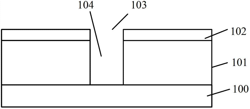
[0089] Step S42, using plasma with a constant duty ratio to etch the stacked structure to form a first etching hole;

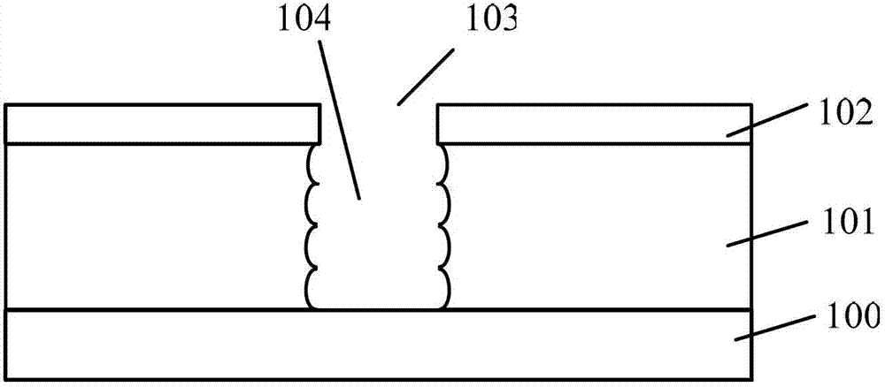
[0090] In step S43 , along the first etching hole, the stack structure is etched with a plasma having a continuously decreasing duty cycle to form a second etching hole, and the first etching hole and the second etching hole form a through hole.

[0091] Figure 15~Figure 17 It is a schematic cross-sectional structure diagram of the formation proc...

no. 4 example

[0110] refer to Figure 18 , Figure 18 It is a schematic flowchart of a method for forming a semiconductor structure according to a fourth embodiment of the present invention, including:

[0111] Step S51, providing a substrate, forming a multi-layer stack structure in which silicon nitride layers and silicon oxide layers are alternately distributed on the substrate, forming a mask layer on the surface of the stack structure, and the mask layer has a surface that exposes the stack structure surface open mouth

[0112] Step S52, using a continuous plasma etching process to etch the stacked structure to form a third etching hole;

[0113] Step S53, then performing plasma etching in which the bias power source outputs bias power in a pulsed manner to the stacked structure along the third etching hole to form a fourth etching hole, a third etching hole and a fourth etching hole form a through hole.

[0114] Figure 19~Figure 21 It is a schematic cross-sectional structure dia...


PUM


Abstract

The invention discloses a method for forming a semiconductor structure, which comprises the following steps: providing a substrate, forming a multi-layer stack structure in which a silicon nitride layer and a silicon oxide layer are alternately distributed on the substrate; carrying out a plasma etching on the stack structure, wherein outputting a bias power in pulse mode by a bias power source, when the bias power source is turned on, etching part of the stack structure to form an etch-hole, when the bias power source is turned off, forming a polymer on the side wall and the bottom of the formed etching hole, repeating the process of turning on the bias power resource and turning off the bias power resource till a through hole is formed. The etching step and the polymer forming step are carried out alternately, after the etch-hole with a depth is etched, correspondingly, the polymer is formed on the side of the etch-hole, subsequently, the formed etch-hole is protected from being over-etched when continuing to etch the stack structure along the etch-hole, so that the finally formed through hole keeps a vertical side wall morphology.

Description

technical field [0001] The invention relates to the field of semiconductor manufacturing, in particular to a method for forming a semiconductor structure. Background technique [0002] With the development of integrated circuits to sub-micron dimensions, the density of devices and the complexity of processes are increasing, and strict control of the process becomes more important. Among them, the through hole is used as the interconnection between the multilayer metal layers and the connection channel between the active area of ​​the device and the external circuit. Due to its important role in the composition of the device structure, the formation process of the through hole has always been a technical skill in the art. personnel's attention. [0003] Figure 1~Figure 3 It is a structural schematic diagram of the existing through-hole forming process. [0004] refer to figure 1 , providing a semiconductor substrate 100, forming a material layer 101 to be etched on the s...

Claims


Application Information

Patent Timeline
Patent Type & Authority Applications(China)
IPC IPC(8): H01L21/768H01L21/311
Inventor 王兆祥梁洁邱达燕
Owner ADVANCED MICRO FAB EQUIP INC CHINA
Why Eureka
Try Eureka