Organic light-emitting diode and method for producing same

An electroluminescent device and electroluminescent technology, which are applied in the fields of electro-solid devices, semiconductor/solid-state device manufacturing, electrical components, etc., can solve the problems of OLED device attenuation, high device operating voltage, and increased device complexity, etc.

Active Publication Date: 2012-10-17
GUAN YEOLIGHT TECH CO LTD +1
View PDF6 Cites 13 Cited by
  • Summary
  • Abstract
  • Description
  • Claims
  • Application Information

AI Technical Summary

Problems solved by technology

As early as 1999, studies by H.Aziz, et al and others showed that the entry of holes into the electron transport layer is an important reason for the attenuation of OLED devices. People have been studying electron transport materials with stable electrochemical properties, but the effect is not satisfactory.
At the same time, it was also proposed to add a hole blocking layer between the light-emitting layer and

Method used


Image

  • Organic light-emitting diode and method for producing same
  • Organic light-emitting diode and method for producing same
  • Organic light-emitting diode and method for producing same

Examples


Embodiment 1-4

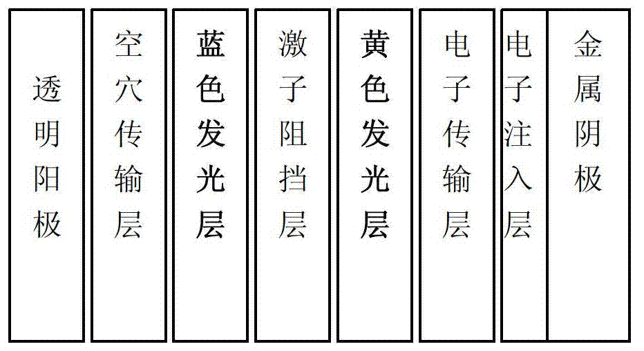
[0091] The organic electroluminescent device provided in this embodiment includes the following layers in sequence: transparent anode, hole transport layer, green light-emitting layer, electron transport layer, electron injection layer, metal cathode, and the materials used in each layer and the composition of each layer. The thickness is:

[0092] ITO(150nm) / TCTA(40nm) / YH-1(30nm): 10%GD / C1(20nm) / LiF(0.5nm) / Al(150nm).

[0093] The specific method for preparing the organic electroluminescent device of this embodiment is as follows:

[0094] A. Use deionized water to ultrasonically clean the glass substrate, place it under an infrared lamp and dry it, and evaporate a layer of ITO anode material on the glass substrate with a film thickness of 150nm;

[0095] B. Place the above-mentioned glass substrate with the anode in a vacuum chamber and evacuate to 1×10 -5 Pa, continue to evaporate the hole transport layer on the above-mentioned anode layer film, such as E3 film, the rate i...

Embodiment 1-5

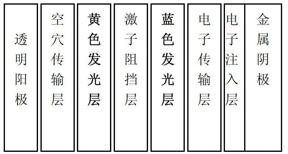
[0100] The organic electroluminescent device provided in this embodiment includes the following layers in sequence: transparent anode, hole transport layer, green light-emitting layer, electron transport layer, electron injection layer, metal cathode, and the materials used in each layer and the composition of each layer. The thickness is:

[0101] ITO (150nm) / E10 (40nm) / YH-2 (30nm): 10%GD / C3 (20nm) / LiF (0.5nm) / Al (150nm).

[0102] The specific method for preparing the organic electroluminescent device of this embodiment is as follows:

[0103] A. Use deionized water to ultrasonically clean the glass substrate, place it under an infrared lamp and dry it, and evaporate a layer of ITO anode material on the glass substrate with a film thickness of 150nm;

[0104] B. Place the above-mentioned glass substrate with the anode in a vacuum chamber and evacuate to 1×10 -5 Pa, continue to evaporate the hole transport layer on the above-mentioned anode layer film, such as E10 film, the ...

Embodiment 1-6

[0109] The organic electroluminescent device provided in this embodiment includes the following layers in sequence: transparent anode, hole transport layer, green light-emitting layer, electron transport layer, electron injection layer, metal cathode, and the materials used in each layer and the composition of each layer. The thickness is:

[0110] ITO(150nm) / E15(40nm) / YH-3(30nm): 10%GD / C4(20nm) / LiF(0.5nm) / Al(150nm).

[0111] The specific method for preparing the organic electroluminescent device of this embodiment is as follows:

[0112] A. Use deionized water to ultrasonically clean the glass substrate, place it under an infrared lamp and dry it, and evaporate a layer of ITO anode material on the glass substrate with a film thickness of 150nm;

[0113] B. Place the above-mentioned glass substrate with the anode in a vacuum chamber and evacuate to 1×10 -5 Pa, continue to evaporate the hole transport layer on the above-mentioned anode layer film, such as E15 film, the rate i...


PUM

PropertyMeasurementUnit
Electron mobilityaaaaaaaaaa

Abstract

The invention provides an organic light-emitting diode which comprises an anode, a hole transport layer, a light-emitting functional layer, an electron transport layer, an electron injection layer and a cathode which are sequentially arranged, wherein the hole transport layer and the electron transport layer are distributed on bipolar materials on the same group through adopting an electron orbit and a hole orbit, and both the hole and electron mobilities of the bipolar materials which are adopted by the hole transport layer and the electron transport layer are between 1*10<-4> and 1*10<-2>cm <2>V<-1> s<-1>. The electron orbit and the hole orbit which are adopted by the diode are distributed on the materials on the same group, the electron transport performance and hole transport mobility which respectively correspond to the hole and the electron transport materials are also similar, so the effective charge compound balance performances are enabled to be similar, and accordingly, the charge compound balance is ensured.

Description

technical field [0001] The invention relates to the technical field of organic electroluminescent devices, in particular to an organic electroluminescent device in which bipolar materials are used for both the transport layer and the main body material. The invention also relates to a preparation method of the organic electroluminescent device. Background technique [0002] Organic electroluminescent devices (OLEDs) can be used in the fields of display and lighting due to their advantages such as ultra-thin, wide viewing angle, and active light emission. Among them, luminous efficiency and lifetime are the main bottlenecks restricting the commercialization of OLEDs. OLED is a technology in which organic semiconductor materials emit light through the injection and recombination of electrons and holes under the action of an electric field. The principle is to use the ITO transparent electrode and the metal electrode as the anode and cathode of the device respectively. Under a...

Claims


Application Information

Patent Timeline
IPC IPC(8): H01L51/54H01L51/50H01L51/56
Inventor 邱勇张国辉董艳波段炼
Owner GUAN YEOLIGHT TECH CO LTD
Why Eureka
Try Eureka