SOI LDMOS device with interface N<+> layer

A semiconductor and interface technology, applied in the direction of semiconductor devices, electrical components, circuits, etc., can solve the problems of low withstand voltage and low withstand voltage, so as to improve the longitudinal withstand voltage, improve the withstand voltage, alleviate the breakdown voltage and on-resistance The contradictory effect between

Active Publication Date: 2014-12-10
NO 24 RES INST OF CETC
View PDF6 Cites 0 Cited by
  • Summary
  • Abstract
  • Description
  • Claims
  • Application Information

AI Technical Summary

Problems solved by technology

[0007] In view of this, in order to solve the problem of low withstand voltage of SOI devices, the present invention proposes an SOI LDMOS semiconductor device with improved withstand voltage capability, which can effectively improve the withstand voltage of the entire device for the shortcoming of low vertical withstand voltage of SOI devices, and its withstand Due to the enhancement of the electric field of the dielectric buried layer and the optimization of the electric field in the top active silicon layer, the voltage is effectively improved compared with the conventional structure SOI device.

Method used


Image

  • SOI LDMOS device with interface N&lt;+&gt; layer
  • SOI LDMOS device with interface N&lt;+&gt; layer
  • SOI LDMOS device with interface N&lt;+&gt; layer

Examples


Embodiment Construction

[0030] The preferred embodiments of the present invention will be described in detail below in conjunction with the accompanying drawings; it should be understood that the preferred embodiments are only for illustrating the present invention, rather than limiting the protection scope of the present invention.

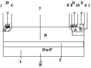
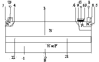
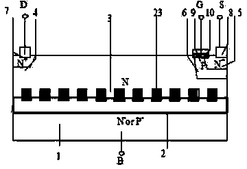
[0031] Figure 7 with interface N + layer SOI LDMOS semiconductor device structure, as shown in the figure: the invention provides a + Layered SOI LDMOS semiconductor devices, including a substrate silicon layer, a dielectric buried layer and an active top layer silicon, the dielectric buried layer is arranged between the substrate silicon layer and the active top layer silicon, and the active top layer silicon includes N-type Silicon layer, P-type silicon layer and N + silicon layer, the N + The silicon layer is disposed on the dielectric buried layer, and the P-type silicon layer is disposed on the N + Above the silicon layer, the N-type silicon layer is disposed ...


PUM


Abstract

The invention discloses an SOI (Semiconductor ON Insulator) LDMOS (Laterally Diffused Metal Oxide Semiconductor) device with an interface N<+> layer, and relates to a semiconductor power device. The SOI LDMOS device comprises a substrate silicon layer, a medium buried layer and active top layer silicon, wherein the medium buried layer is arranged between the substrate silicon layer and the active top layer silicon; and the active top layer silicon is divided into an N-type silicon layer, a P-type silicon layer and an N<+> silicon layer from the surface of a semiconductor to the medium buried layer. According to the invention, as the N<+> silicon layer is arranged between the medium buried layer and the active top layer silicon, when the device is in a reverse blocking state, exhausted high-concentration ionized donor at the interface part enhances the electric field of the medium buried layer, the distribution of the electric field in the active top layer silicon is effectively modulated, and accordingly, the longitudinal voltage resistance and the transverse voltage resistance of the device are effectively improved. Meanwhile, the P-type silicon layer in the active top layer silicon can adjust the RESURF (Reduced SURface Field) condition of the device and relieve the contradiction between the breakdown voltage and the on resistance of the device.

Description

technical field [0001] The invention relates to a semiconductor power device, in particular to a device with an interface N + layers of SOI LDMOS semiconductor devices. Background technique [0002] Silicon on Insulator (Semiconductor On Insulator or SOI) is a semiconductor substrate material with a new structure developed in the 1980s. Its unique structural characteristics overcome the shortcomings of many conventional bulk silicon materials and give full play to silicon integrated circuit technology. The potential of silicon, known as the silicon integration technology of the 21st century, has received extensive attention and in-depth research from many experts and scholars at home and abroad. [0003] SOI high-voltage integrated circuit (High Voltage Integrated Circuit, HVIC) integrates microelectronics technology, SOI technology and power electronics technology. It has developed rapidly in recent years and has become a very important emerging branch in the field of powe...

Claims


Application Information

Patent Timeline
Patent Type & Authority Patents(China)
IPC IPC(8): H01L29/06H01L29/78
Inventor 胡盛东罗俊谭开洲徐学良王健安秦国林唐昭焕陈文锁
Owner NO 24 RES INST OF CETC
Why Eureka
Try Eureka