

Light emitting diode (LED) based on silicon substrate through hole technology flip chip and manufacturing process of LED
A light-emitting diode and flip-chip technology, applied in electrical components, circuits, semiconductor devices, etc., can solve the problems of difficult LED packaging devices, poor contact of gold wire solder joints, falling off, etc., to improve reliability and uniformity of light output, Compact size and uniform phosphor layer
- Summary
- Abstract
- Description
- Claims
- Application Information
AI Technical Summary
Problems solved by technology
Method used
Image

Examples
Embodiment 1
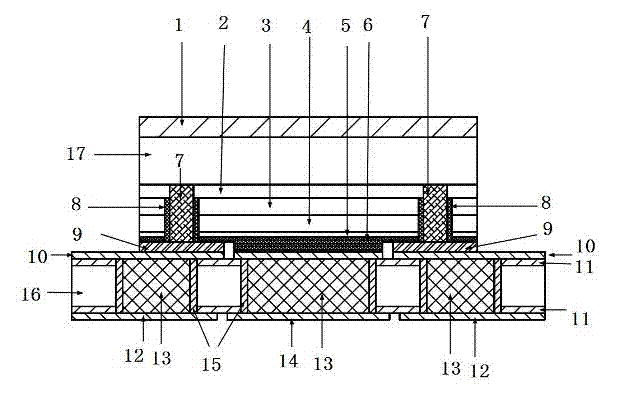
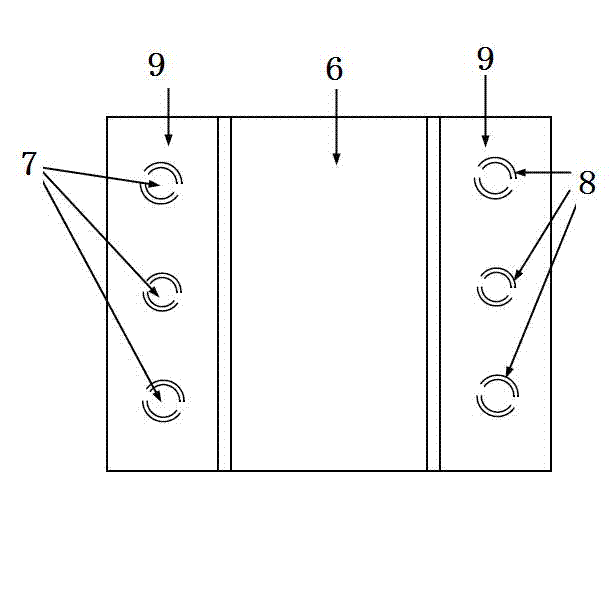
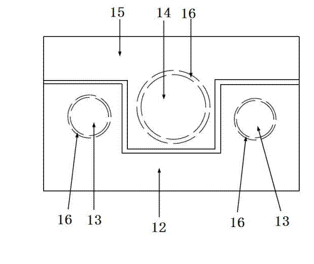
[0021] see figure 1 , figure 2 , image 3 , the flip-chip light-emitting diode based on silicon substrate through-hole technology, including: fluorescent layer 1, n-type current spreading layer 2, light-emitting layer 3, p-type current spreading layer 4, metal reflective layer 5, p-type electrode pad 6. Metal through hole 7, insulating layer 8, n-type electrode pad 9, silicon substrate circuit layer 10, silicon substrate insulating layer 11, silicon substrate negative electrode pad 12, silicon substrate electrode metal through hole 13, silicon substrate positive electrode Pad 14, silicon substrate through-hole insulating layer 15, chip sapphire substrate 17, silicon substrate 16; it is characterized in that n-type current spreading layer 2, light-emitting layer 3, p-type current spreading layer are grown on sapphire substrate 17 in sequence 4. The metal reflective layer 5, the p-type electrode pad 6; the n-type current spreading layer 2 is connected to the n-type electrode ...
Embodiment 2
[0023] The preparation process of the above light-emitting diode is as follows:
[0024] First, on the sapphire substrate 17, an n-type current spreading layer 2, a light-emitting layer 3, a p-type current spreading layer 4, a metal light-reflecting layer 5, and a p-type electrode pad 6 are sequentially fabricated to form a light-emitting diode chip; through etching technology Or the laser technology is used to make through holes on the light-emitting diode chip and the silicon substrate, and after making the insulating layer 8 and the through hole insulating layer 15 of the silicon substrate respectively on the surrounding wall of the through hole, carry out the making of the metal through hole 7 and the electrode metal through hole 13; then Carry out the making of metal layer n-type electrode pad 9, silicon substrate line layer 10, silicon substrate negative electrode pad 12, silicon substrate positive electrode pad 14 on chip electrode surface and silicon substrate surface r...
Embodiment 3
[0026] This embodiment is basically the same as Embodiment 2, and the special features are as follows:
[0027] The sapphire substrate 17 is thinned and surface microstructured to produce microstructures with a diameter of 20-500nm, a pitch of 100-1500nm, and a height of 20-200nm (or laser lift-off); the silicon substrate 16 is etched by etching technology or Electrode metal through holes 13 are produced by laser technology, and the n-type electrode pad 9 and the p-type electrode pad 6 are led to the bottom surface of the silicon substrate 16; , or use transparent ceramic technology to make the fluorescent layer 1 made of ceramic fluorescent chip technology, and roughen the upper surface of the fluorescent chip or fluorescent film (nano- and micron-level microstructure), and then directly cover the light-emitting surface of the light-emitting diode ; The n-type electrode pad 9 and the p-type electrode pad 6 are connected to the silicon substrate circuit layer 10 by eutectic te...
PUM
| Property | Measurement | Unit |
|---|---|---|
| Diameter | aaaaa | aaaaa |
| Thickness | aaaaa | aaaaa |
Abstract
Description
Claims
Application Information