Supercharge Your Innovation With Domain-Expert AI Agents!

Thyristor with deep energy level doping element drift area

A technology of doping elements and deep-level impurities, which is applied in the field of semiconductor power devices, can solve the problems of slow hole extraction by gate electrode control signal, thyristor turn-off failure, and accelerated gate electrode extraction, so as to reduce high-temperature leakage current and accelerate Turn-off process, effect of improving turn-off characteristics

Inactive Publication Date: 2012-11-14
UNIV OF ELECTRONIC SCI & TECH OF CHINA +1
View PDF1 Cites 2 Cited by
  • Summary
  • Abstract
  • Description
  • Claims
  • Application Information

AI Technical Summary

Problems solved by technology

When the metal grid 2 is applied with a turn-off trigger current, it can accelerate the extraction of holes from the gate electrode to the P-type base region 5. When the holes in the P+ anode region are pulled to the gate electrode by the positive electric field, the trigger current of the gate electrode accelerates the gate Electrode pairs hole extraction, reducing α NPN , so that the sum of the common base current amplification factors of the parasitic NPN transistor and the parasitic PNP transistor is α NPN +α PNP <1, so that the thyristor cannot maintain its self-turn-on state, so the thyristor turns off
Although the thyristor has many performance advantages and can be widely used in the field of electronic circuits, the turn-off process of the thyristor is a very difficult process. Due to the large anode leakage current of the thyristor and the positive temperature coefficient, as the temperature rises, the anode The leakage current rises sharply; the gate trigger current drive circuit is also difficult to control, which makes the process of extracting holes by the gate electrode control signal very slow and even leads to the failure of the thyristor to turn off

Method used


Image

  • Thyristor with deep energy level doping element drift area
  • Thyristor with deep energy level doping element drift area
  • Thyristor with deep energy level doping element drift area

Examples


Embodiment Construction

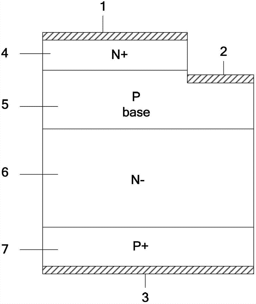
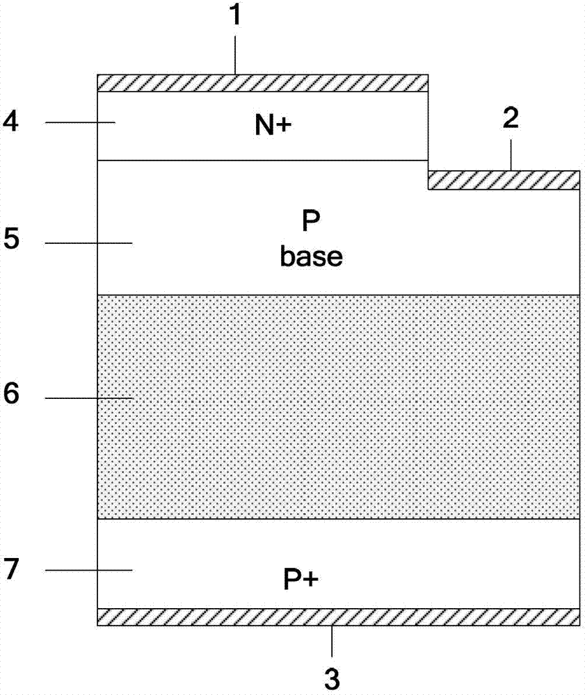
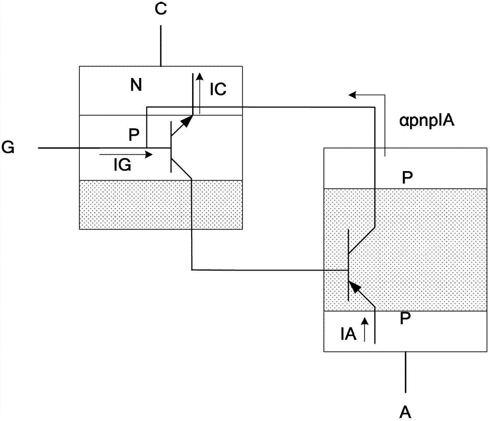
[0015] A thyristor with a deep-level doped element drift region, its cell structure is as follows figure 2 As shown, it includes a metallized cathode 1, a polysilicon gate electrode 2, a metallized anode 3, an N+ active region 4, a P-type base region 5, an N-drift region 6, and a P+ anode region 7; the metallized anode 3 is located in the P+ anode region 7, the N-drift region 6 is located above the P+ anode region 7, the P-type base region 5 is located above the N-drift region 6, and the P-type base region 5 is connected to the polysilicon gate electrode 2; the N+ active region 4 is located on the P-type base region Above the region 5, and connected to the metallized cathode 1; the N-drift region 6 is doped with deep-level impurity elements (specific doping elements include: sulfur, selenium, tellurium, gold or platinum).

[0016] It should be further explained that the N-drift region 6 can be fully or partially doped with deep-level impurity elements (that is, the implantati...


PUM


Abstract

The invention discloses a thyristor with a deep energy level doping element drift area, and belongs to the technical field of semiconductor power devices. According to the thyristor, deep energy level doping elements (sulphur, selenium, tellurium, gold or platinum) are doped into an N-drift area (6) of the conventional thyristor; the ionization degrees of the deep energy level doping elements are increased along with the raising of the temperature so as to result in the increase of impurity concentration, so that alpha PNP (plug-and-play) of the PNP transistor under high temperature is effectively reduced; and therefore, the influence of the temperature on high-temperature anode leakage current can be reduced, the high-temperature leakage current is reduced, and the power consumption of the transistor is further reduced; when the device is turned on / off, triggering current is turned off by a gate electrode to quicken the extraction of a hole, so that alpaha NPN of a parasitic NPN transistor is reduced, the impurity concentration of the drift area is raised so as to cause the decrease of the alpha PNP, the process of alpha NPN+aPNP is quickened, the self-maintaining effect of the transistor is disappeared, and the device is easily turned off.

Description

technical field [0001] The invention belongs to the technical field of semiconductor power devices, and relates to a thyristor, especially a thyristor doped with deep-level elements in a drift region. Background technique [0002] Thyristors have the advantages of high current and high voltage, and are widely used in rectification, non-contact electronic switches, inverter and frequency conversion circuits and systems. A traditional thyristor, the structure of which is as figure 1 As shown, when the positive voltage is applied to the metal anode 3 and the trigger current is applied to the metal grid 2 to provide the base current for the parasitic NPN transistor, the parasitic NPN transistor will be turned on accordingly, and the parasitic NPN transistor will also provide the parasitic PNP transistor The base current, so that the parasitic PNP transistor is also turned on, and the turn-on of the parasitic PNP further provides the base current for the parasitic NPN, thus form...

Claims


Application Information

Patent Timeline
IPC IPC(8): H01L29/74H01L29/12
Inventor 李泽宏李巍陈伟中张蒙张金平任敏张波
Owner UNIV OF ELECTRONIC SCI & TECH OF CHINA
Features
  • R&D
  • Intellectual Property
  • Life Sciences
  • Materials
  • Tech Scout
  • Unparalleled Data Quality
  • Higher Quality Content
  • 60% Fewer Hallucinations
Learn More