Preparation method of transmission electron microscopy sample for in-situ electrical testing

A transmission electron microscope sample and electrical technology, which is applied in the preparation of test samples and other directions, can solve the problems of difficulty in preparing TEM samples for in-situ electrical testing, and achieves the effect of solving the problem of electrical connection, simple preparation process, and reducing the difficulty of preparation.

Active Publication Date: 2015-02-04
INST OF MICROELECTRONICS CHINESE ACAD OF SCI
View PDF1 Cites 0 Cited by
  • Summary
  • Abstract
  • Description
  • Claims
  • Application Information

AI Technical Summary

Problems solved by technology

[0003] The present invention aims at the difficulty of preparing TEM samples for in-situ electrical testing by existing TEM sample preparation methods, and provides a method for preparing transmission electron microscope samples for in-situ electrical testing

Method used


Image

  • Preparation method of transmission electron microscopy sample for in-situ electrical testing
  • Preparation method of transmission electron microscopy sample for in-situ electrical testing
  • Preparation method of transmission electron microscopy sample for in-situ electrical testing

Examples


Embodiment 1

[0027] The preparation method of the transmission electron microscope sample that the present invention is used for in-situ electric test comprises the following steps:

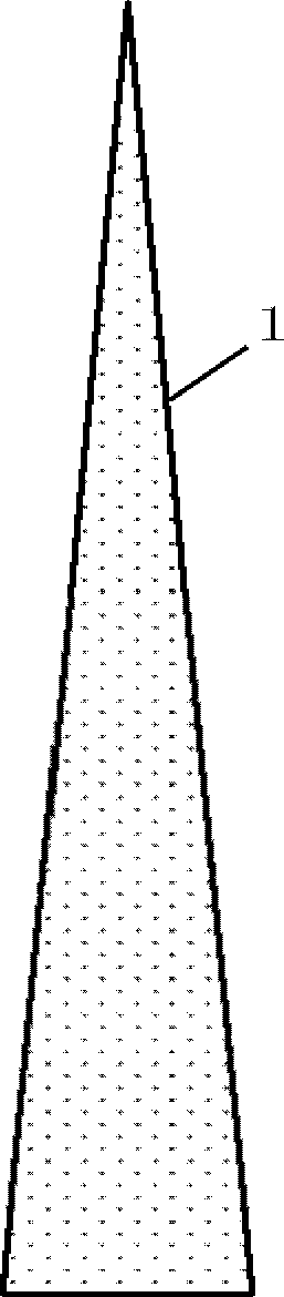
[0028] Step 1. Using the FIB etching process, the top tip of the metal probe is flattened to form a platform with a flat surface, which is used as a preparation substrate for semiconductor devices at both ends.

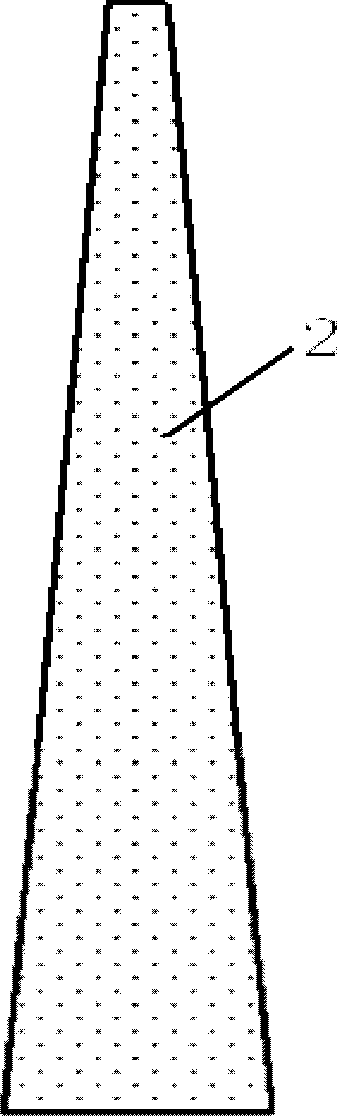
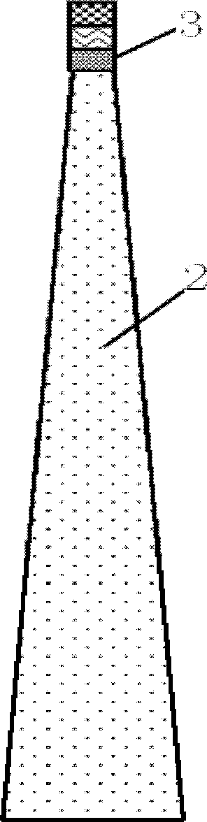
[0029] Such as figure 1 As shown, it is the metal probe 1 before treatment. The top of the W needle with a diameter of 3 mm is processed into a circular table with a diameter of 10 μm by using the FIB etching process, and by adjusting the acceleration voltage and the etching rate during the FIB ion etching process Current to ensure the flatness of the surface of the circular table, such as figure 2 Shown is a metal probe 1 forming a flat surface platform 2 .

[0030] Step 2: Using a semiconductor thin film preparation process, a semiconductor device with both ends is prepared on the top platform o...

Embodiment 2

[0040] In this example, the same process steps as in Example 1 were used to prepare TiN / HfO on the Pt probe 2 / TiN RRAM, TiN and HfO 2 The thin film materials are respectively obtained by means of magnetron sputtering and atomic layer deposition, and the thicknesses are 50nm / 10nm / 50nm respectively.


PUM

PropertyMeasurementUnit
diameteraaaaaaaaaa
lengthaaaaaaaaaa
diameteraaaaaaaaaa

Abstract

The invention relates to a preparation method of transmission electron microscopy samples for in-situ electrical testing. The method comprises the following steps: cutting a top needle point of a metal probe to be flat so as to form a platform with a flat surface; preparing a two-end semiconductor device on the top platform of the metal probe; depositing a protective layer on the top of the formed two-end semiconductor device; thinning the two-end semiconductor device by using the protective layer as a mask so as to form a thin sheet; cutting the thin sheet of the two-end semiconductor device to form a plurality of independent TEM testing samples. The invention solves the electrical connection problem of TEM samples and an in-situ electrical testing TEM sample rod, avoids the step of sample extraction and transfer to a Cu net in routine TEM sample preparation by FIB, reduces the difficulty for sample preparation, improves the success rate of sample preparation, and greatly reduces the cost of sample preparation.

Description

technical field [0001] The invention relates to a preparation method of a transmission electron microscope sample, in particular to a preparation method of a transmission electron microscope sample used for in-situ electrical testing, and belongs to the technical field of electron microscope sample preparation. Background technique [0002] Transmission Electron Microscopy (TEM, Transmission Electron Microscopy) is one of the important technical means for the research and characterization of material structure, its spatial resolution can reach the picometer level, and it can observe the local fine structure of the material at the atomic scale and analyze the material structure. It is an important means of material science research to analyze the local components of the material. With the development of electron microscopy technology, there have been some new TEM supporting devices that provide in-situ application of heat, force, electricity, light and other excitations, and ...

Claims


Application Information

Patent Timeline
Patent Type & Authority Patents(China)
IPC IPC(8): G01N1/32
Inventor 刘琦刘明龙世兵吕杭炳李颖涛王艳谢常青
Owner INST OF MICROELECTRONICS CHINESE ACAD OF SCI
Why Eureka
Try Eureka