Photonic crystal beam splitter

A photonic crystal and beam splitter technology, applied in the field of semiconductor optics, can solve problems such as small manufacturing tolerance, and achieve the effects of large manufacturing tolerance, simple and mature manufacturing process, and flexible design

Inactive Publication Date: 2012-11-21
SHANGHAI INST OF MICROSYSTEM & INFORMATION TECH CHINESE ACAD OF SCI
View PDF2 Cites 3 Cited by
  • Summary
  • Abstract
  • Description
  • Claims
  • Application Information

AI Technical Summary

Problems solved by technology

[0008] The technical problem to be solved by the present invention is to provide a photonic crystal beam splitter, which is used to overcome the problems that the existing photonic crystal Y beam splitter requires a relatively accurate exposure process and small manufacturing tolerances.

Method used


Image

  • Photonic crystal beam splitter
  • Photonic crystal beam splitter
  • Photonic crystal beam splitter

Examples


Embodiment Construction

[0031] In order to make the object, technical solution and advantages of the present invention clearer, the present invention will be further described in detail below in conjunction with the accompanying drawings.

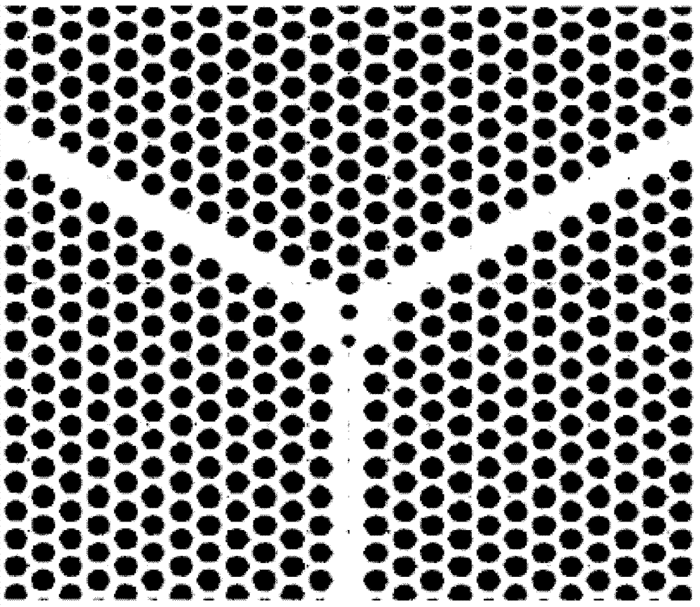
[0032] In general, the transmission of light beams can be guided by introducing defects as channels inside photonic crystals. However, photonic crystals also have a unique property - the self-collimation effect. Based on this effect, there is no need to introduce any defects inside the photonic crystal, and the light beam itself can overcome the diffraction and divergence and collimate forward. This characteristic is derived from the dispersion relationship of photonic crystals. In addition to being able to automatically collimate and transmit, self-collimated beams also have zero-crossing effects, angle insensitivity effects, and insensitivity to photonic crystal structure precision.

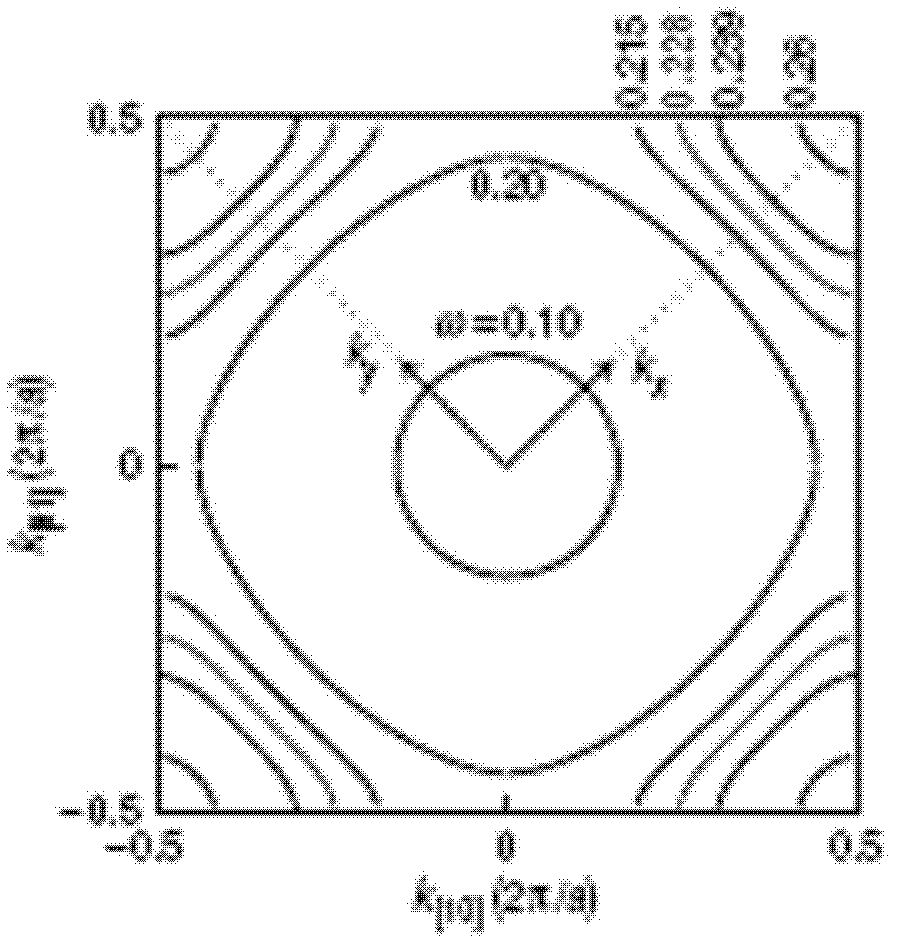
[0033] figure 2 It is the isofrequency diagram of the first energy band of ...


PUM


Abstract

The invention relates to a photonic crystal beam splitter which realizes the beam splitting and propagating of the inputted optical signals by the auto-collimation effect of the SOI (silicon on insulator) based two-dimensional flat air-hole photonic crystal, belonging to the field of optical technology of the semiconductors. The photonic crystal beam splitter comprises an SOI substrate, an air hole area and an SOI stripe-shaped waveguide; the air hole area is formed on the top-layer silicon of the SOI substrate by etching silicon; the SOI stripe-shaped waveguide is used for connecting the air hole area with the external optical fiber or other devices; the air holes formed by etching silicon in the air hole area are arrayed on the top-layer silicon of the SOI substrate like square crystal lattices; the depth of the air holes is equal to the thickness of the top-layer silicon of the SOI substrate; and the SOI stripe-shaped waveguide is the inputting waveguide of the beam-splitter and keeps a certain distance with both the air hole area and two borders which are parallel to the inputting waveguide. The length of the beam splitting area of the beam splitter can be controlled with 10mum, thus the overall length of the device is reduced greatly, and the structure is more compact. In addition, the photonic crystal beam splitter has large preparation tolerance and more flexible design and can be more widely used for the future photonic chip.

Description

technical field [0001] The invention relates to a photonic crystal beam splitter used in the fields of optical communication, optical calculation, optical sensing, optical measurement and the like, in particular to a structure of a photonic crystal beam splitter made of SOI material, which belongs to the technical field of semiconductor optics. Background technique [0002] In the past half century, silicon-dominated microelectronics technology has made remarkable achievements, which has greatly promoted the arrival of the golden age of information technology. The monopoly position of silicon in the market and the huge advantages in technology attract people to continuously develop miniaturized and integrated silicon-based photonic devices to realize large-scale integrated photonic chips. [0003] Silicon-on-Insulator (Silicon-on-Insulator, SOI) is a unique silicon-based material system. The use of this material to make optoelectronic devices is conducive to compatibility wi...

Claims


Application Information

Patent Timeline
Patent Type & Authority Applications(China)
IPC IPC(8): G02B6/122G02B6/136
Inventor 王曦杨志峰武爱民甘甫烷林旭林李浩
Owner SHANGHAI INST OF MICROSYSTEM & INFORMATION TECH CHINESE ACAD OF SCI
Why Eureka
Try Eureka