
Single ended differential gain amplifier with configurable radio frequency broadband gain

A single-ended to differential, gain amplifier technology, applied in differential amplifiers, DC-coupled DC amplifiers, gain control, etc. Issues such as when signals of different bands are input at the same time

Active Publication Date: 2012-11-21
杭州中科微电子有限公司
View PDF3 Cites 23 Cited by
  • Summary
  • Abstract
  • Description
  • Claims
  • Application Information

AI Technical Summary

Problems solved by technology

[0004] There are many disadvantages in the prior art RF gain amplifiers: First, the RF amplifiers with traditional structure are all fixed gain, which is not suitable for high dynamic input requirements with strong interference or weak signals
Second, RF amplifiers with traditional structures work in a narrow-band environment, which cannot meet the requirements of simultaneous input of signals of different bands.
Third, none of the traditional radio frequency amplifiers can convert single-ended signals into differential circuits, and an additional balun component that converts single-ended signals into differential signals is required outside the chip, which not only increases the cost of the overall solution, but also increases the input The output chip pins reduce the stability of the signal and increase the difficulty of the overall design
Fourth, there are limitations and defects in the driving capability of the output buffer circuit
Single-ended to differential gain configurable RF wideband gain amplifier gain step ratio is large is single-ended to differential gain configurable gain coarse adjustment in RF wideband gain amplifier

Method used


Image

  • Single ended differential gain amplifier with configurable radio frequency broadband gain
  • Single ended differential gain amplifier with configurable radio frequency broadband gain
  • Single ended differential gain amplifier with configurable radio frequency broadband gain

Examples


no. 1 example

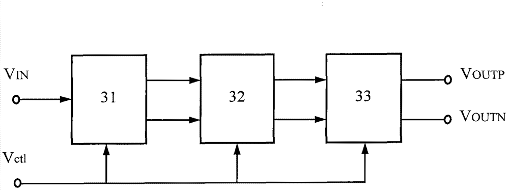
[0062] FIG. 3 shows a block diagram of a circuit configuration of a radio frequency broadband gain amplifier with configurable gain from single-ended to differential in an embodiment of the present invention. In conjunction with Fig. 3, the configuration of the gain configurable structure in the present invention is illustrated: the input signal V IN Enter the single-ended input end of the single-ended to differential circuit 31 with configurable gain, and the single-ended to differential circuit 31 with configurable gain is connected in parallel by single-ended to differential amplifier circuits 311 to 314, and the single-ended to differential amplifier circuits 311 to 314 are connected in parallel The input signal is converted from a single-ended signal to a differential signal, the switches 315-418 control the access of the variable gain stages 311-314, the differential output signal passes through the control switch pair 35-318, and the access gain can be configured to the ...

no. 2 example

[0064] Figure 4 A circuit connection block diagram of a single-ended to differential gain configurable radio frequency broadband gain amplifier and a baseband digital processing module chip control signal of an application embodiment of the present invention is given. The baseband chip provides three sets of control words to control the single-ended to differential gain and configure the radio frequency broadband gain amplifier circuit, which are Vctl1, Vctl2 and Vctl3, Vctl1 controls the gain to control the single-ended to differential circuit 31, Vctl2 controls the gain to configure the broadband circuit 32, Vctl3 controls the gain configurable buffer driver circuit 33 .

[0065] The differential output signal of the RF wideband gain amplifier 41 with configurable gain from single-ended to differential is sent to the external baseband digital processing module 42 through the differential output end of the buffer drive circuit 33 with configurable gain, and the baseband digi...

no. 3 example

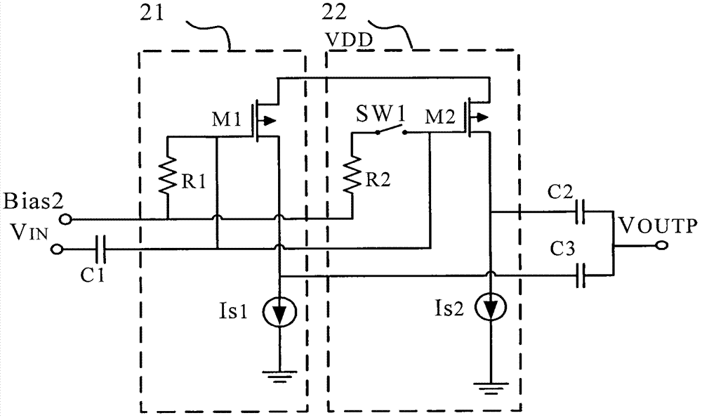
[0069] Figure 5-7 Schematic diagrams of a gain-configurable single-ended-to-differential amplifier circuit, a gain-configurable broadband amplifier circuit, and a gain-configurable buffer drive circuit of an embodiment of the present invention are given.

[0070] Figure 5 The schematic diagram of the single-end to differential amplifier circuit in the single-end to differential circuit with configurable gain is given in . The single-end to differential amplifier circuit is a cascode circuit structure with adjustable amplification. The input signal V IN Through the DC blocking capacitors C1 and C2, they are respectively input to the input amplifier tubes M1 and M2. The input amplifier tubes M1 and M2 amplify the amplitude of the input signal with the same amplification, and adjust the phase of the input signal with the opposite phase. In the input amplifier tube M1, The differential output V of the parallel load of L1 and R3 of M2 and the parallel load of L2 and R4 OUTN and...


PUM


Abstract

The invention discloses a single ended differential gain amplifier with a configurable radio frequency broadband gain. The gain amplifier comprises a single ended differential circuit with a configurable gain, a broadband amplifying circuit with the configurable gain and a buffer driving circuit with the configurable gain which are sequentially connected in series. Gain control ends of the circuits are connected with a gain control signal from an outer digital base band processing module to form a gain value of the single ended differential gain amplifier with the configurable radio frequency broadband gain in combination, according to the control of each circuit at a set fixed step pitch, fine adjustment on the gain is implemented, thus a range of the broadband signal output by the differential conforms to a range value of a set signal, and strong disturbance is effectively restrained. Since the strong detection and processing capability of a digital processing module chip of the outer base band is good for a gain control mode, the gain control is enabled not to be affected from temperature, process, noise and the like, and more precise and flexible control can be realized. The control range of the gain is a summation of the maximum gain control ranges of the three circuits with the configurable gains, so that the gain amplifier is suitable for application of the high dynamic input with strong disturbance or weak signal, and is suitable for a radio frequency chip with multiple frequencies and multiple modes of a single ended broadband radio frequency signal input.

Description

Contents of the invention [0001] The invention belongs to the technical field of radio frequency communication, and relates to a single-end to differential amplifier circuit, in particular to a single-end to differential gain configurable radio frequency broadband gain amplifier, which is used in a radio frequency receiver, and it can realize the amplified output of small signals, At the same time, the suppression of strong interference signals can be realized, and the amplification and reduction of input signals are controlled by the baseband digital processing module chip. Background technique [0002] In recent years, with the continuous emergence of new technologies in the field of information technology and the continuous progress of technology, the RF front-end and baseband digital processing module chips of various receiver systems have achieved great development. The development of chips with fixed small gain or large gain is becoming more and more mature, but becaus...

Claims


Application Information

Patent Timeline
Patent Type & Authority Applications(China)
IPC IPC(8): H03G3/20H03F3/45
Inventor 何晓丰莫太山
Owner 杭州中科微电子有限公司
Learn More