Manufacturing method for back contact crystalline silicon solar cell

A technology for a solar cell and a manufacturing method, applied in the field of solar cells, can solve the problems of increasing the production cost of the cell, reducing the parallel resistance of the cell, and being prone to leakage, so as to reduce the laser isolation process, reduce the risk of leakage, and reduce the cost of equipment. Effect

Inactive Publication Date: 2012-11-28
CSI CELLS CO LTD
View PDF4 Cites 0 Cited by
  • Summary
  • Abstract
  • Description
  • Claims
  • Application Information

AI Technical Summary

Problems solved by technology

[0013] In the existing manufacturing process, in the diffusion junction step, a conductive layer that short-circuits the P-N junction will be formed between the backlight surface of the solar cell and the conductive hole, which greatly reduces the parallel resistance of the cell and is prone to leakage, so The conductive layer between the P-N junction needs to be removed by laser isolation step
However, the use of laser isolation may cause new leakage paths in solar cells, resulting in a decrease in the performance of the cells. In addition, the laser damages the cells themselves, and debris may appear during the laser isolation process, which increases the production of cells. cost

Method used


Image

  • Manufacturing method for back contact crystalline silicon solar cell
  • Manufacturing method for back contact crystalline silicon solar cell
  • Manufacturing method for back contact crystalline silicon solar cell

Examples


Embodiment 1

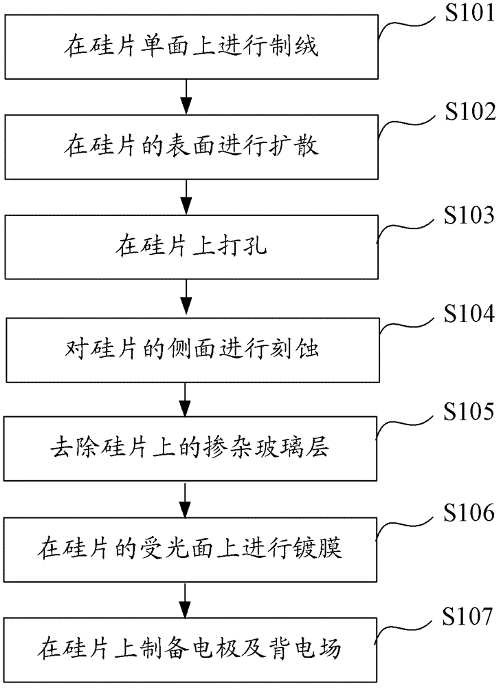
[0052] Please refer to figure 1 , figure 1 The flow chart of the method for manufacturing the back contact crystalline silicon solar cell provided in the first embodiment, as shown in figure 1 As shown, the method includes the following steps:

[0053] Step S101: performing texturing on one side of the silicon wafer to form a surface structure;

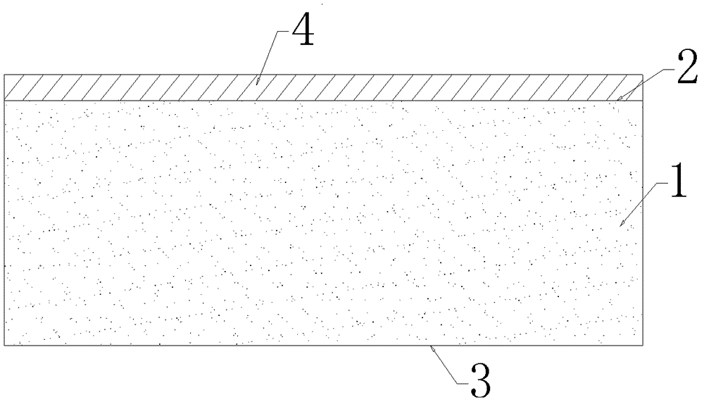
[0054]In the embodiment of the present invention, texturing is selected to be carried out on one side of the silicon wafer 1. The purpose of texturing is to form an uneven structure on the originally bright silicon wafer surface through a chemical reaction to prolong the propagation path of light on the surface, thereby Improve the absorption of light by the silicon wafer. The schematic diagram of the structure of the silicon wafer after texturing is as follows: figure 2 As shown in the figure, 1 is a silicon wafer, 2 is a light-receiving surface, 3 is a backlight surface, and 4 is a suede surface. In addition, oil and metal imp...

Embodiment 2

[0073] Please refer to Figure 8 , Figure 8 A flow chart of a method for manufacturing a back-contact crystalline silicon solar cell provided in Example 2, as shown in Figure 8 As shown, the method includes the following steps:

[0074] Step S201: performing texturing on both surfaces of the silicon wafer to form a surface structure;

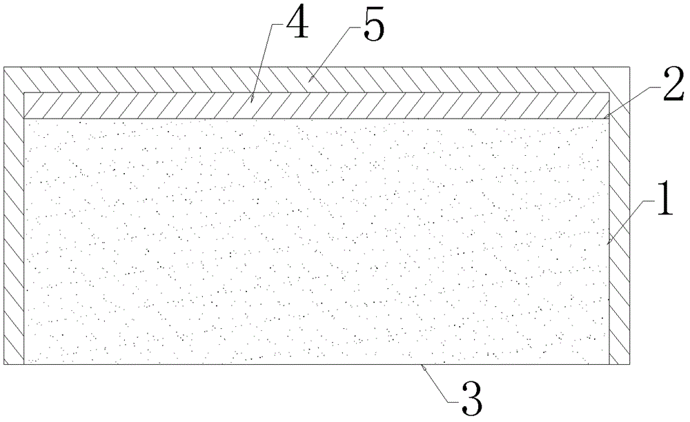
[0075] The schematic diagram of the structure of the silicon wafer after texturing is as follows: Figure 9 As shown, the suede 4 is formed on both surfaces of the silicon wafer 1 in the figure.

[0076] Step S202: Diffusion on the surface of the silicon wafer to form a P-N junction;

[0077] The schematic diagram of the structure of the silicon wafer after diffusion is shown in Figure 10 As shown in Figure 5, there are emitter junctions diffused on both surfaces and side surfaces of the silicon wafer 1.

[0078] Compared with the steps S101-S103, the above two steps are only that texturing and diffusion are carried out on both sides of...


PUM


Abstract

The invention discloses a manufacturing method for a back contact crystalline silicon solar cell. The manufacturing method comprises the following steps of: performing texturing and diffusion on the surface of a semiconductor substrate; reserving through holes in the semiconductor substrate after the diffusion; etching the semiconductor substrate with the through holes; removing a doped glass layer from the etched semiconductor substrate; coating a film on the illuminated surface of the semiconductor substrate from which the doped glass layer is removed; and preparing electrodes and a back surface field on the film-coated semiconductor substrate to obtain the back contact crystalline silicon solar cell. According to the method, the surface of the semiconductor substrate is diffused, and the through holes are reserved in the semiconductor substrate after the diffusion, so that the inner walls of the through holes cannot be diffused, namely emitter junctions in the through holes are avoided. Compared with the prior art, the method has the advantages of eliminating a laser isolation procedure, reducing the electric leakage risks of the cell and greatly lowering the fragmentation rate of the cell. In addition, the laser isolation procedure is eliminated, so that a process is simple, equipment cost is reduced, and industrial production is facilitated.

Description

technical field [0001] The present application relates to the technical field of solar cells, in particular to a method for manufacturing back-contact crystalline silicon solar cells. Background technique [0002] A solar cell, also known as a photovoltaic cell, is a semiconductor device that converts the sun's light energy directly into electrical energy. Because it is a green product, does not cause environmental pollution, and is a renewable resource, solar cells are a new energy source with broad development prospects in today's energy shortage situation. At present, more than 80% of solar cells are made of crystalline silicon materials. Therefore, the preparation of high-efficiency crystalline silicon solar cells is of great significance for large-scale utilization of solar power generation. The main grid line, the positive electrode and the negative electrode are all located on the backlight side of the cell, which greatly reduces the shading rate of the light-receivi...

Claims


Application Information

Patent Timeline
Patent Type & Authority Applications(China)
IPC IPC(8): H01L31/18
CPCH01L31/1804H01L31/068H01L31/0682H01L31/02245Y02E10/547Y02P70/50
Inventor 章灵军张凤吴坚王栩生
Owner CSI CELLS CO LTD
Why Eureka
Try Eureka