

Solar cell having back surface field structures and manufacturing method thereof
A technology for solar cells and manufacturing methods, which is applied in the directions of final product manufacturing, sustainable manufacturing/processing, circuits, etc., can solve the problems of reduced conversion efficiency, structural damage of the dielectric layer 12, affecting the quality and function of the dielectric layer 12, and the like, Achieve the effect of avoiding damage and improving conversion efficiency
- Summary
- Abstract
- Description
- Claims
- Application Information
AI Technical Summary
Problems solved by technology
Method used
Image

Examples
Embodiment Construction
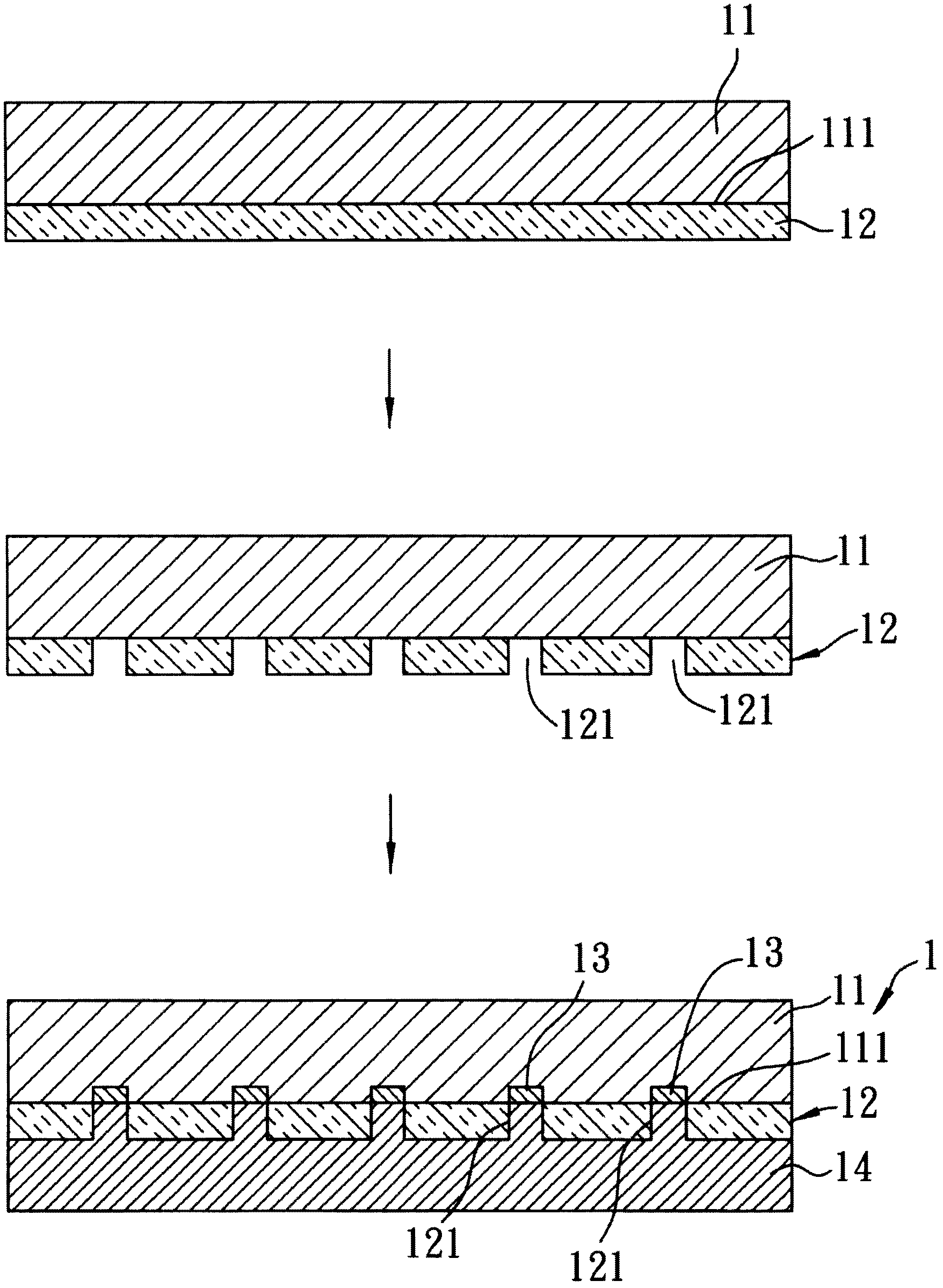
[0029] The present invention will be described in detail below with reference to the accompanying drawings and embodiments. It should be noted that in the following description, similar elements are denoted by the same numerals.
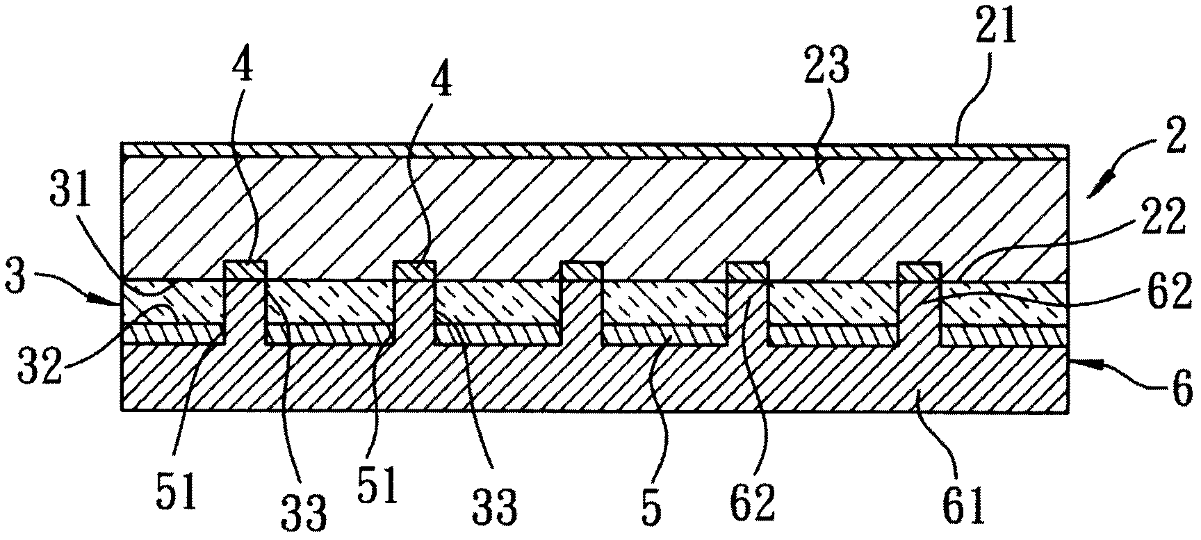
[0030] refer to figure 2 , The first preferred embodiment of the solar cell with a back electric field structure of the present invention includes: a wafer 2 , a dielectric layer 3 , a plurality of back electric field structures 4 , a metal barrier layer 5 and a conductive adhesive layer 6 .
[0031] The wafer 2 is used for converting light energy into electrical energy, and includes a light incident surface 21 and a back surface 22 opposite to the light incident surface 21 . The wafer 2 actually includes a substrate 23 with the back surface 22, an emitter layer formed on the substrate 23, an anti-reflection film and other film layers. The substrate 23 in this embodiment is a p-type silicon substrate 23, and the emitter layer For the n-type emitter...
PUM
| Property | Measurement | Unit |
|---|---|---|
| thickness | aaaaa | aaaaa |
Abstract
Description
Claims
Application Information