Method for manufacturing N electrode of GaN-based light-emitting diode (LED)

A manufacturing method and electrode technology, applied in circuits, electrical components, semiconductor devices, etc., can solve the problems of serious absorption of metal electrodes, large refractive index difference, low light extraction efficiency, etc., to improve light extraction efficiency, facilitate wire bonding, simple craftsmanship

Inactive Publication Date: 2012-12-19
YANGZHOU ZHONGKE SEMICON LIGHTING
View PDF4 Cites 12 Cited by
  • Summary
  • Abstract
  • Description
  • Claims
  • Application Information

AI Technical Summary

Problems solved by technology

The main factors affecting the external quantum efficiency of GaN-based LEDs are not only the low light extraction efficiency due to the large refractive index difference between GaN materials and air, but also the absorption of light by metal electrodes is also very serious.
As we all know, conventional LED chips need positive and negative electrodes connected to make them emit light. Correspondingly, positive and negative wiring pads need to be made on the chip, usually made of gold. Gold absorbs blue and green light greatly, which greatly affects the light output efficiency.

Method used


Image

  • Method for manufacturing N electrode of GaN-based light-emitting diode (LED)
  • Method for manufacturing N electrode of GaN-based light-emitting diode (LED)

Examples


Embodiment Construction

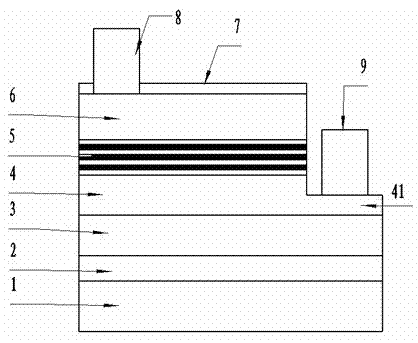
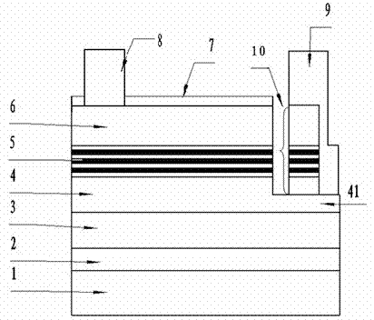
[0009] A method for making the N electrode in a GaN-based LED of the present invention, such as figure 2 shown, including the following steps:

[0010] Step 1: Fabricate GaN epitaxial wafers: use metal organic chemical vapor deposition (MOCVD) to sequentially grow a low-temperature GaN buffer layer 2 with a thickness of 1 μm, an undoped GaN layer 3 with a thickness of 2 μm, and a thickness of An N-GaN layer 4 of 3 μm, a multi-quantum well light-emitting layer 5 with a thickness of 200 nm and a P-GaN layer 6 with a thickness of 700 nm form a GaN epitaxial wafer. Wherein, the semiconductor substrate 1 may be any one of sapphire, silicon, silicon carbide or metal.

[0011] Step 2: ICP (Inductively Coupled Plasma) Mesa Etching of GaN:

[0012] For conventional LEDs, one side of the GaN epitaxial wafer is etched by ICP to remove all the P-GaN layer 6, the multi-quantum well light-emitting layer 5 and the vertical part of the N-GaN layer 4 on one side to form N-GaN 41, such as f...


PUM


Abstract

The invention discloses a method for manufacturing the N electrode of a GaN-based light-emitting diode (LED), and relates to a method for manufacturing the N electrode in an LED manufacturing process. During inductively coupled plasma tabletop etching, only a part of a transverse P-GaN layer, a part of a transverse multi-quantum well luminous layer and a part of a longitudinal N-GaN layer on one side of a GaN epitaxial wafer are removed, a part of the transverse P-GaN layer, a part of the transverse multi-quantum well luminous layer and a part of the longitudinal N-GaN layer are reserved, and form an N tabletop, and the N tabletop, a sidewall on one side of the N tabletop and the N-GaN layer are evaporated by using the metal CrPtAu of the N electrode. A process is simple, stable and reliable, a new process step is not required to be added, routing is facilitated, and the luminous efficiency of the GaN-based LED can be effectively improved.

Description

technical field [0001] The invention relates to the technical field of optoelectronic device manufacturing, in particular to a method for manufacturing an N electrode in the manufacturing process of a gallium nitride (GaN)-based light-emitting diode (LED). Background technique [0002] With the development of epitaxial growth technology and multi-quantum well structure, the internal quantum efficiency of GaN-based LEDs has been greatly improved. At present, the internal quantum efficiency of GaN-based LEDs can reach more than 70%, but the external quantum efficiency of LED chips is usually Only about 40%. The main factors affecting the external quantum efficiency of GaN-based LEDs are not only the low light extraction efficiency due to the large refractive index difference between GaN materials and air, but also the absorption of light by metal electrodes is also very serious. As we all know, conventional LED chips need positive and negative electrodes connected to make the...

Claims


Application Information

Patent Timeline
Patent Type & Authority Applications(China)
IPC IPC(8): H01L33/00H01L33/40H01L33/38
Inventor 李璟詹腾张溢冯亚萍
Owner YANGZHOU ZHONGKE SEMICON LIGHTING
Why Eureka
Try Eureka