

Nanowire-based transparent conductors and methods of patterning same
A technology of transparent conductors and nanostructures, applied in the direction of nanotechnology, nanotechnology, nanotechnology, etc. for information processing, can solve the problem of low conductivity value, high optical absorption, lack of chemical stability and long-term stability of conductive polymers And other issues
- Summary
- Abstract
- Description
- Claims
- Application Information
AI Technical Summary
Problems solved by technology
Method used
Image

Examples
preparation example Construction
[0163] Deposition of nanowires and preparation of transparent conductors
[0164] Accordingly, in certain embodiments, described herein are methods of making a transparent conductor comprising: depositing a plurality of metal nanowires distributed in a fluid on a substrate; and forming metal nanowires on the substrate by drying the fluid. line network layer.
[0165] Metal nanowires can be prepared as described above. Metal nanowires are typically dispersed in a liquid to facilitate deposition. It should be understood that, as used herein, "deposition" and "coating" are used interchangeably. Any non-corrosive liquid in which the metal nanowires can form a stable dispersion (also referred to as a "metal nanowire dispersion") can be used. Preferably, the metal nanowires are dispersed in water, alcohols, ketones, ethers, hydrocarbons or aromatic solvents (benzene, toluene, xylene, etc.). More preferably, the liquid is volatile and has a boiling point of no more than 200°C, ...
Embodiment 1
[0397] Synthesis of silver nanowires
[0398] Silver nanowires were synthesized by reduction of silver nitrate dissolved in ethylene glycol in the presence of poly(vinylpyrrole tetrachloride) (PVP), as described e.g. in Y. Sun, B. Gates, B. Mayers , and Y. Xia's "Crystalline silver nanowires by soft solution processing" ("Crystalline silver nanowires by soft solution processing") Nanoletters, (2002), 2 (2) 165-168 described in the "polyol" method. In an improved process described in US application Ser. No. 11 / 766,552 to Cambrios Technologies Corporation, more uniform silver nanowires are produced at higher yields than the traditional "polyol" process. This application is hereby incorporated by reference in its entirety.
Embodiment 2
[0400] Preparation of transparent conductors
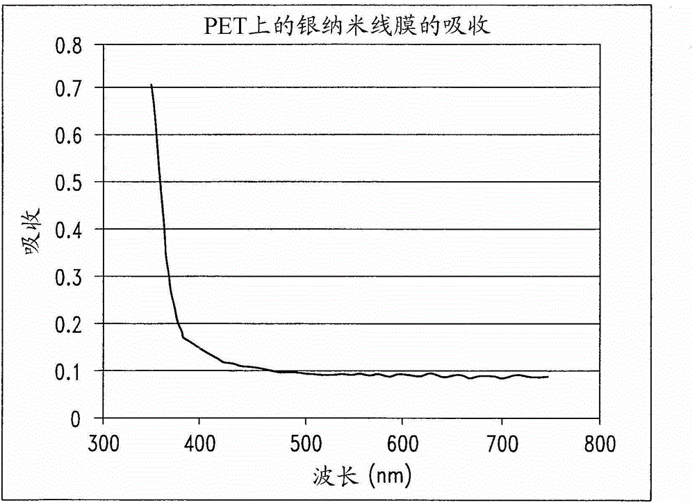
[0401] Autoflex EBG5 polyethylene terephthalate (PET) with a thickness of 5 μm was used as the substrate. PET substrates are optically transparent insulators. The light transmittance and haze of the PET substrates are shown in Table 2. Light transmittance was measured using the method in ASTM D 1003 unless otherwise stated.
[0402] First, an aqueous dispersion of silver nanowires is prepared. The silver nanowires have a width of about 70 nm to 80 nm and a length of about 8 μm. The concentration of silver nanowires (AgNW) was about 0.5% w / v of this dispersion, resulting in an optical density of about 0.5 (measured on a Molecular Devices Spectra Ma×M2 plate reader). The dispersion was then coated on a PET substrate by precipitating the nanowires onto the substrate. Other coating techniques may be used, such as flow metered by a narrow channel, die flow, flow over an inclined plane, etc., as will be appreciated by those skilled...
PUM
| Property | Measurement | Unit |
|---|---|---|
| Boiling point | aaaaa | aaaaa |
| Viscosity | aaaaa | aaaaa |
| Surface resistivity | aaaaa | aaaaa |
Abstract
Description
Claims
Application Information