Method and system for cleaning electronic material

An electronic material and cleaning system technology, applied in the field of cleaning systems, can solve problems such as high operating costs and unstable cleaning power, achieve high cleaning power and shorten the time required for cleaning

Inactive Publication Date: 2012-12-26
KURITA WATER INDUSTRIES LTD
View PDF6 Cites 9 Cited by
  • Summary
  • Abstract
  • Description
  • Claims
  • Application Information

AI Technical Summary

Problems solved by technology

Therefore, when SPM is used in the resist removal process using a single-wafer cleaning device, there is a disadvantage that if the reagent is recycled, the cleaning power is unstable, and due to the large consumption of sulfuric acid and hydrogen peroxide, it is difficult to operate High cost and produces a lot of waste liquid

Method used


Image

  • Method and system for cleaning electronic material

Examples


Embodiment 1)

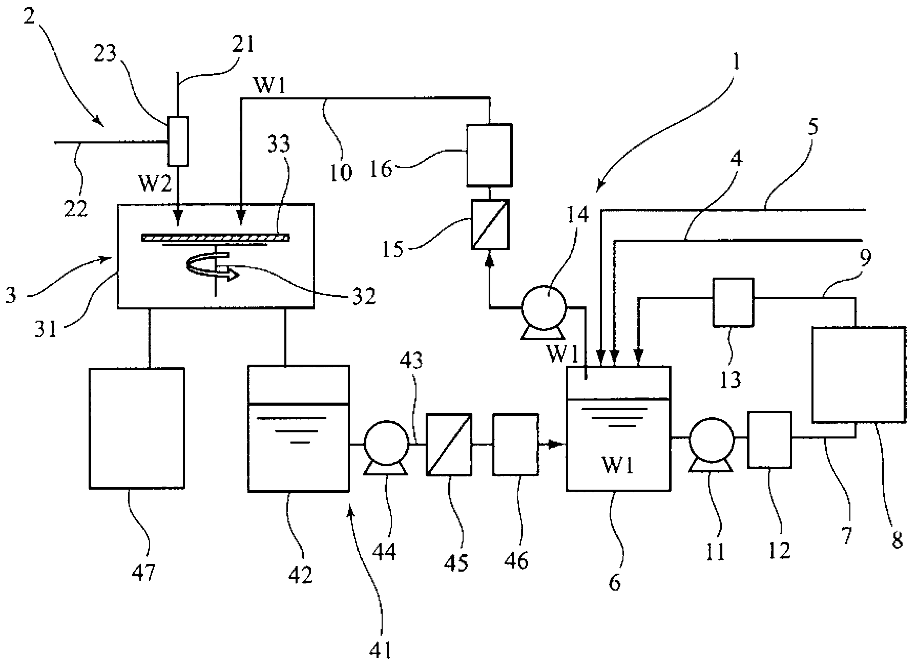
[0078] use figure 1 The test device shown was used to perform a test of stripping and removing the resist of a 12-inch wafer, which was patterned with a KrF excimer laser and implanted with As ions at a concentration of 1E+15 [atoms / cm 2 ] formed with a resist.

[0079] The test conditions are, while adjusting the concentration of sulfuric acid to 92% by mass and the concentration of persulfuric acid to 10g / L (converted to S 2 o 8 ) is electrolyzed with the electrolytic reaction device 8 on the left and right sides, so that about 30 L of the sulfuric acid (functional reagent W1) is possessed in the functional reagent storage tank 6, and the functional reagent W1 is supplied while being heated by the heater 16 by the reagent supply pump 14. In the single-chip cleaning device 3. The functional reagent W1 is heated to 180° C. by the heater 16 and supplied onto the silicon wafer 33 fixed in the single-wafer cleaning apparatus 3 at 160 to 170° C. to perform a reagent cleaning st...

Embodiment 2)

[0081] As in Example 1, except that the time of the reagent cleaning process was set to 30 seconds and the time of the wet cleaning process was set to 30 seconds, the cleaning was repeated twice, and then spin drying was performed, and the resist was carried out in the same manner. Agent stripping treatment. As a result, it took 4 minutes including spin drying from the start of supply of the functional reagent W1 to the completion of the resist stripping process.


PUM

PropertyMeasurementUnit
thicknessaaaaaaaaaa

Abstract

An electronic material cleaning system includes a chemical cleaning means, a wet cleaning means and a single-wafer cleaning apparatus. The chemical cleaning means comprises a functional chemical storage tank and an electrolytic reaction apparatus connected to the functional chemical storage tank via a concentrated sulfuric acid electrolysis line. The functional chemical storage tank can supply a functional chemical to the single-wafer cleaning apparatus via a functional chemical supply line. The wet cleaning means comprises a pure water supply line, a nitrogen gas supply line connected to a nitrogen gas source and an internal mixing type two-fluid nozzle connected respectively to the pure water supply line and the nitrogen gas supply line. Droplets generated from a nitrogen gas and ultrapure water can be sprayed from the tip of the two-fluid nozzle.

Description

technical field [0001] The present invention relates to the effective use of resists, etc. Cleaning method and cleaning system for strip removal. Background technique [0002] The semiconductor manufacturing process includes a process of locally implanting metal ions as impurities on the surface of the semiconductor wafer. In this step, a resist made of a photosensitive resin material or the like is patterned as a mask material in order to prevent implantation into an undesired portion, and ions of the same concentration are also implanted on the resist surface. Since the resist after ion implantation is a useless product in terms of production, a resist removal process for peeling and removing it from the wafer surface is performed. [0003] In such a resist removal process, after the resist is ashed by an ashing device, it is transported to a cleaning device, and resist residues are removed by a cleaning solution. However, when an ashing process is performed using an as...

Claims


Application Information

Patent Timeline
Patent Type & Authority Applications(China)
IPC IPC(8): H01L21/304B08B3/08B08B3/10G03F7/42H01L21/027
CPCB08B3/04H01L21/31133H01L21/67051G03F7/423H01L21/02052H01L21/02057H01L21/6708
Inventor 山川晴义床嶋裕人
Owner KURITA WATER INDUSTRIES LTD
Why Eureka
Try Eureka