

Novel three-junction thin-film solar cell and production method thereof
A solar cell, three-junction technology, applied in circuits, photovoltaic power generation, electrical components, etc., to achieve the effect of improving photoelectric conversion rate and low manufacturing cost
- Summary
- Abstract
- Description
- Claims
- Application Information
AI Technical Summary
Problems solved by technology
Method used
Image

Examples
Embodiment Construction
[0016] Below in conjunction with accompanying drawing, the present invention is described in further detail:
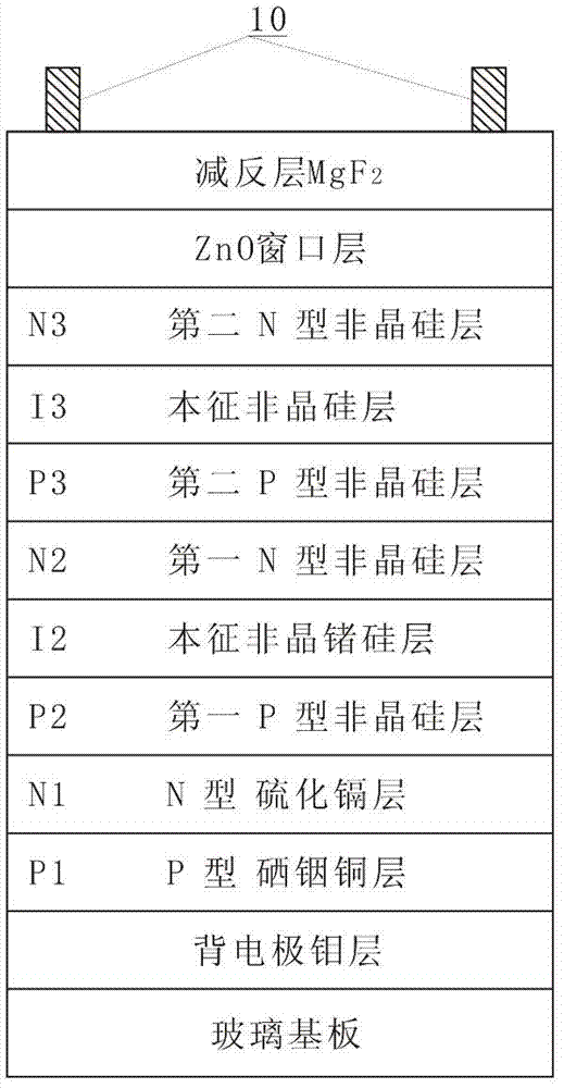
[0017] Such as figure 1 As shown, the novel triple-junction thin-film solar cell of the present invention includes a glass substrate, a back electrode molybdenum layer, a multi-junction cell unit, a zinc oxide window layer and an anti-reflection layer of magnesium fluoride arranged in sequence from bottom to top, and magnesium fluoride The antireflection layer is provided with an aluminum gate electrode 10; the multi-junction battery unit includes three junctions, which are indium selenium copper junction, amorphous germanium silicon junction and amorphous silicon junction from bottom to top, and the selenium indium copper junction is P1 and N1, The amorphous germanium silicon junctions are P2, I2 and N2, and the amorphous silicon junctions are P3, I3 and N3. Specifically, the indium selenium copper junction includes a P-type indium selenium copper layer and an N-type...
PUM
| Property | Measurement | Unit |
|---|---|---|
| Thickness | aaaaa | aaaaa |
| Thickness | aaaaa | aaaaa |
| Thickness | aaaaa | aaaaa |
Abstract
Description
Claims
Application Information