Nitride light emitting diode and manufacturing method thereof

A technology of light-emitting diodes and nitrides, applied in chemical instruments and methods, from chemically reactive gases, crystal growth, etc., can solve the problems of reducing the carrier capture ability, reducing the radiation recombination efficiency, and reducing the injection efficiency. Uniform heat source distribution and luminous intensity, reducing Auger recombination and improving recombination efficiency

Inactive Publication Date: 2014-03-19
TIANJIN SANAN OPTOELECTRONICS
View PDF4 Cites 12 Cited by
  • Summary
  • Abstract
  • Description
  • Claims
  • Application Information

AI Technical Summary

Problems solved by technology

Traditional GaN-based LEDs generally use InGaN / GaN structures, such as figure 1 As shown, the GaN-based epitaxial layer grown along the C-plane on sapphire and silicon carbide substrates has spontaneous polarization and piezoelectric polarization, resulting in severe bending of the energy bands of quantum wells and quantum barriers, which greatly reduces the carrier trapping ability, the injection efficiency becomes lower, and the radiative recombination efficiency decreases

Method used


Image

  • Nitride light emitting diode and manufacturing method thereof
  • Nitride light emitting diode and manufacturing method thereof
  • Nitride light emitting diode and manufacturing method thereof

Examples


Embodiment 1

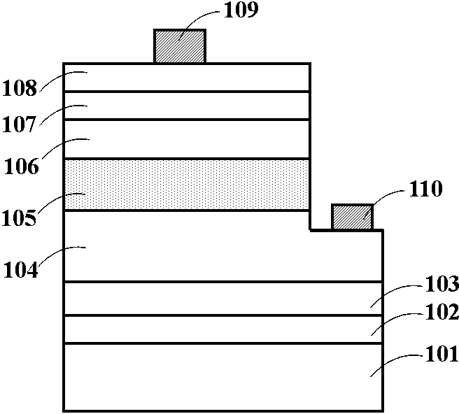
[0038] Such as figure 2 As shown, the nitride light-emitting diode includes: a sapphire substrate 201, a low-temperature buffer layer 202, an undoped GaN layer 203, an n-type GaN layer 204, an active region 205, a p-type electron blocking layer 206, and a p-type GaN layer 207 , p-type highly doped GaN contact layer 208 , p-electrode 209 and n-electrode 210 . The following describes in detail in conjunction with the preparation method.

[0039] First grow a low-temperature buffer layer 202 on a sapphire substrate 201, then grow a non-doped GaN layer 203 with a thickness of 1 μm, and then form a Si-doped layer 203 with a Si doping concentration of 1.5×10 on the non-doped GaN layer 203. 19 cm -3 The n-type GaN layer 204, followed by growing the multi-quantum well active region 205, and then growing the p-type Al 0.15 Ga 0.85 The N layer is used as the p-type electron blocking layer 206, and the Mg doping concentration is 5×10 19 cm -3 After the epitaxial growth of the p-ty...

Embodiment 2

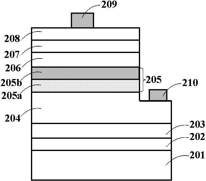
[0042] The difference between this embodiment and embodiment 1 is: the front M of the active region is opposite to the Al 0.10 In 0.16 Ga 0.74 Al and In compositions in N / GaN quantum wells are graded. Such as image 3 As shown, a nitride light-emitting diode includes: a sapphire substrate 301, a low-temperature buffer layer 302, an undoped GaN layer 303, an n-type GaN layer 304, an active region 305, a p-type electron blocking layer 306, and a p-type GaN layer 307 , p-type highly doped GaN contact layer 308 , p-electrode 309 and n-electrode 310 . Among them, 4 cycles of Al x In 1-x-y Ga y The values ​​of Al composition x in N / GaN multiple quantum well 305a are 0.025, 0.05, 0.075 and 0.1 from bottom to top, and correspondingly, the values ​​of In composition 1-x-y are 0.04, 0.08, 0.12 and 0.16 from bottom to top .

Embodiment 3

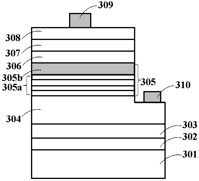
[0044] Such as Figure 4 As shown, compared with the previous embodiment, the difference is that the quantum well energy band design of this embodiment is different, Al x In 1-x-y Ga y N-well bandgap width ( E g ) minimum value is larger than the bandgap width of the InGaN well. Specifically, Al x In 1-x-y Ga y The bandgap width of the N well is 2.9~3.4eV, and the bandgap width of the InGaN well is 2.3~2.8eV. Thanks Al x In 1-x-y Ga y N-well bandgap width ( E g ) > Bandgap width of InGaN well ( E g ), avoiding that the light generated by the epitaxially grown InGaN well is first epitaxially grown Al x In 1-x-y Ga y The efficiency is reduced due to the absorption of the N well; in addition, the shallower Al x In 1-x-y Ga y The blocking effect of the N well on the return electrons will be better.


PUM


Abstract

The invention discloses a nitride light emitting diode and a manufacturing method thereof. The structure at least comprises a substrate, an n type nitride layer, an active area and a p type nitride layer. The active area comprises M pairs of AlxIn1-x-yGayN / GaN quantum wells and N pairs of InGaN / GaN quantum wells. Electronic reflux and a polarization effect are improved. Composite efficiency of a quantum well area and a density of two-dimension electron gas at an interface are increased. Photoelectric conversion efficiency of the light emitting diode is increased too. Simultaneously, an endurance capacity of the LED to static electricity is enhanced and an electrical property of the LED is improved.

Description

technical field [0001] The invention relates to the field of semiconductor optoelectronic device preparation, in particular to the preparation technology of nitride semiconductor LED. Background technique [0002] GaN-based light-emitting diodes are widely used in daily life. Compared with traditional light sources, LEDs have the advantages of long life, high luminous efficiency, low energy consumption, and small size. It is an important trend in the development of modern lighting. [0003] LED luminous efficiency is one of the most important indicators to measure the quality of LED devices, and the multi-quantum well (MQW) structure is the key to achieve high-efficiency luminescence. Traditional GaN-based LEDs generally use InGaN / GaN structures, such as figure 1 As shown, there are spontaneous polarization and piezoelectric polarization in GaN-based epitaxial layers grown along the C-plane on sapphire and silicon carbide substrates, resulting in severe bending of the energ...

Claims


Application Information

Patent Timeline
Patent Type & Authority Applications(China)
IPC IPC(8): H01L33/06H01L33/32H01L33/14H01L33/00
CPCH01L33/06H01L33/32C30B25/16C30B29/403H01L33/007
Inventor 陈沙沙张东炎刘晓峰王良均王笃祥
Owner TIANJIN SANAN OPTOELECTRONICS
Why Eureka
Try Eureka